

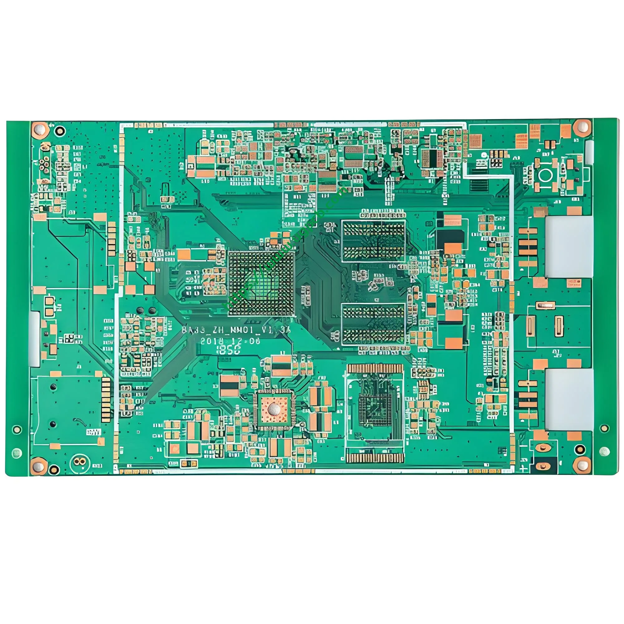
Product Overview: What Is an OSP Antioxidant PCB Circuit Board?
An OSP antioxidant PCB circuit board uses Organic Solderability Preservatives (OSP) as its copper surface finish. This process deposits an ultra-thin organic film on bare copper surfaces. The film prevents oxidation during storage and assembly. During soldering, the flux quickly dissolves the OSP film. This exposes clean copper for reliable solder joints.
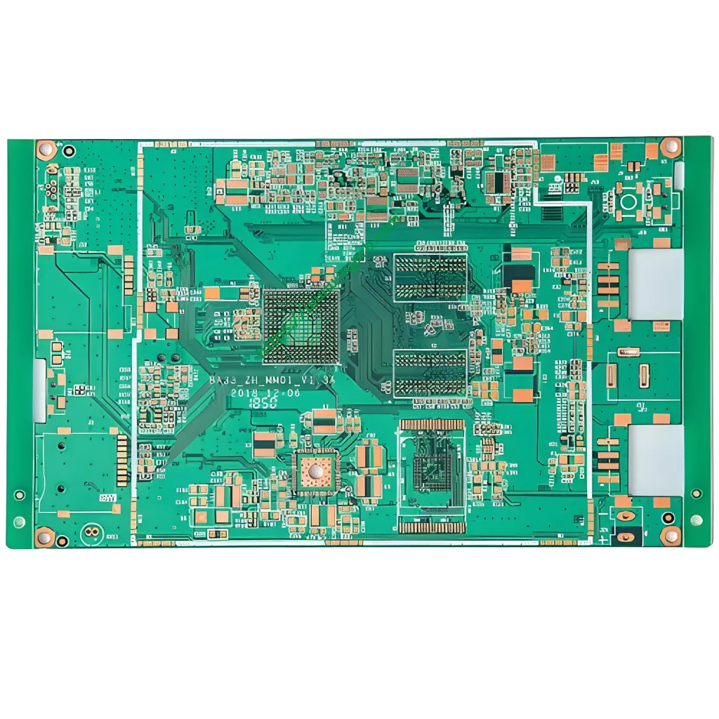
UGPCB’s OSP antioxidant PCB circuit board uses FR-4 glass epoxy laminate as the base material. It features 35μm (1 oz) copper foil, 1.6mm board thickness, and dimensions of 68.36 × 34.6mm. The minimum finished hole size is 0.45mm. Minimum trace width is 0.15mm and minimum spacing is 0.20mm. The product fully complies with IPC-6012E (rigid printed board qualification and performance) and IPC-4555 (high-temperature OSP performance) specifications.
This double-sided OSP PCB serves consumer electronics, communication equipment, and industrial controls. It works best where cost sensitivity and surface flatness matter most.
Scientific Product Classification
Based on international PCB classification systems, this product falls into these categories:
| Classification Dimension | Category |
|---|---|
| Substrate Material | FR-4 epoxy glass fabric rigid PCB |
| Number of Layers | Double-sided (two-layer circuitry) |
| Surface Finish | OSP (Organic Solderability Preservatives) antioxidant |
| Flammability Rating | UL 94 V-0 |
| IPC Performance Class | Class 2 (dedicated service electronic products) |
| Copper Foil Thickness | 1 oz (35μm) standard copper |
| Board Thickness | 1.6mm standard rigid board |
| Hole Type | Through-hole compatible with SMT |
Key Technical Parameters Explained
Substrate: FR-4 Epoxy Glass Fabric
FR-4 is the most common rigid substrate in the PCB industry. “FR” means flame-retardant. “4” indicates epoxy resin combined with glass fabric that meets UL 94 V-0 flammability standards. UL 94 V-0 requires vertical specimens to self-extinguish within 10 seconds after two 10-second flame applications. No flaming drips may ignite cotton.

The glass transition temperature (Tg) measures heat resistance. Standard FR-4 Tg ranges from 130–140°C. Mid-Tg FR-4 reaches 150–160°C. High-Tg FR-4 exceeds 170°C. This product uses standard FR-4 with Tg ≥ 130°C (IPC-4101/21 compliant). This meets the thermal shock demands of reflow soldering (peak temperatures 240–260°C).
Copper Foil Thickness: 35μm (1 oz)
Copper thickness determines current-carrying capacity. This product uses 35μm copper foil, known as 1 oz copper (1 oz/ft² ≈ 35μm). According to IPC-2221, 1 oz copper at 10°C temperature rise carries approximately:
- 0.15mm (6 mil) trace width: 0.5–0.7A
- 0.20mm (8 mil) trace width: 0.8–1.0A
The 35μm copper thickness is the most common standard for double-sided PCBs. It balances cost, current capacity, and manufacturing yield.
Board Dimensions: 68.36 × 34.6mm
The finished board measures 68.36mm × 34.6mm. This compact size suits tight electronic modules. Small PCBs demand tighter precision—dimensional tolerances typically stay within ±0.15mm (IPC-6012 Class 2).
Minimum Finished Hole Size: 0.45mm
0.45mm is the minimum plated through-hole (PTH) diameter. This hole size is a standard in the industry. It ensures reliable plating (aspect ratio approximately 3.6:1 with 1.6mm board thickness). The hole size accommodates most DIP components and standard SMT pad designs.
PCB Thickness: 1.6mm
1.6mm is the most common board thickness in PCB manufacturing. It provides excellent mechanical strength and flexural rigidity. It matches standard connectors and sockets perfectly.
Trace Width and Spacing: 0.15mm / 0.20mm
This product offers minimum trace width of 0.15mm (about 6 mils) and minimum spacing of 0.20mm (about 8 mils). According to IPC classification, these dimensions fall into Class 2 (dedicated service electronic products). This precision meets most medium-density PCB designs, including MCU control boards, power management modules, and interface converter boards.
How OSP Antioxidant Process Works
The OSP process grows an ultra-thin organic film on clean bare copper through chemical adsorption. The OSP film mainly consists of alkyl benzimidazole compounds (azole-based). Film thickness typically ranges from 0.2–0.5μm.
Protection Mechanism
The OSP film protects copper surfaces through three mechanisms:
- Physical barrier – The organic film forms a dense molecular layer. It blocks oxygen and moisture from contacting the copper surface.
- Chemical adsorption – Active groups in OSP molecules bond chemically with copper atoms. This creates strong adhesion.
- Selective protection – The OSP film covers only copper areas. It does not affect solder mask or other non-metallic regions.
Behavior During Soldering
During SMT reflow, temperatures reach 190–230°C. The flux’s active ingredients decompose and dissolve the OSP film. This exposes clean copper underneath. Solder directly contacts bare copper and forms intermetallic compounds (IMC). This creates reliable electrical connections. The OSP film completely decomposes with no residue after soldering.
Key Performance Characteristics
Based on IPC-TM-650 test methods:
| Characteristic | Typical Value / Requirement | Reference Standard |
|---|---|---|
| OSP Film Thickness | 0.2–0.5μm | IPC-4555 |
| Solder Wetting Angle | ≤30° (after 1 reflow) | IPC-TM-650 2.4.1 |
| Solder Spread Ratio | ≥80% | IPC-TM-650 2.4.1 |
| Oxidation Protection (ambient) | ≥6 months | IPC-4555 |
| Contact Resistance Change | ≤10% (after 6 months storage) | IPC-TM-650 |
OSP Antioxidant PCB Manufacturing Process
OSP antioxidant PCB manufacturing follows strict process controls. Every step affects final quality and reliability.
Front-End Processes (Substrate Preparation & Circuit Patterning)
- Material Cutting – Cut FR-4 copper-clad laminate to size
- Drilling – CNC drilling with 0.45mm minimum hole size
- Electroless Copper / Electroplating – Metallize hole walls for layer-to-layer connection
- Circuit Pattern Transfer – Dry film / wet film exposure and development
- Etching – Remove unwanted copper to create 0.15mm trace / 0.20mm spacing circuitry
- Solder Mask Printing – Apply green or other colored solder mask ink
- Pre-Clean – Remove oxides and contaminants before surface finish
OSP Coating Process (Core Process)
The typical OSP coating flow:
Degreasing → Double Water Rinse → Micro-Etching → Double Water Rinse → Acid Pickling → DI Water Rinse → OSP Film Formation → Air Drying → DI Water Rinse → Final Drying
- Micro-Etching – Removes copper oxides and creates a uniform microscopically rough surface. This promotes OSP film growth.
- OSP Film Formation – Immerse the PCB in OSP chemistry (alkyl benzimidazole, organic acids, copper chloride, and deionized water). The film grows through chemical adsorption on copper surfaces.
- Film Thickness Control – Precise control is critical. Too thin means poor heat resistance. Too thick hinders flux action and solder flow.
Back-End Processes
- Routing – CNC routing to final dimensions
- Electrical Testing – Flying probe or fixture testing
- Final Inspection – Visual inspection and film thickness sampling
- Vacuum Packaging – Moisture-proof and oxidation-proof packaging
Product Features and Core Advantages
Excellent Surface Flatness
The OSP film is only 0.2–0.5μm thick. It forms through chemical adsorption with uniform thickness and a smooth surface. This preserves the original copper foil flatness. It is ideal for fine-pitch SMT components (such as 0.4mm and below pitch QFP, QFN packages).
Superior Solderability
The OSP film dissolves quickly in flux during reflow. This exposes fresh copper for reliable IMC formation. The OSP process supports both through-hole (THT) and surface-mount (SMT) soldering.
Cost-Effective
OSP uses no precious metals (gold, silver, palladium). Material and processing costs are lower than ENIG, immersion silver, or immersion tin. For high-volume production like consumer electronics, OSP offers exceptional cost competitiveness.
Environmentally Compliant
OSP uses organic compounds. It contains no lead, mercury, cadmium, or hexavalent chromium. It fully meets RoHS 2.0 requirements. Waste treatment costs and complexity are also lower than metal finishing processes.
Short Processing Time
OSP coating is simple and fast. It needs no complex plating equipment or long deposition times. Compared to ENIG (which takes hours), OSP completes surface finishing in 30–60 minutes per batch. This significantly reduces lead times.
Design Guidelines and Important Considerations
Design for Manufacturing (DFM) Rules
Based on this product’s process capabilities:
| Design Parameter | Product Capability | Recommended Design Value |
|---|---|---|
| Minimum Trace Width | 0.15mm | ≥0.15mm (signal traces) |
| Minimum Spacing | 0.20mm | ≥0.20mm |
| Minimum Hole Size | 0.45mm | ≥0.45mm |
| Board Thickness | 1.6mm | 1.6mm (standard) |
OSP Process Limitations and Mitigations
OSP offers many benefits but has inherent limitations:
- Limited Shelf Life – OSP film protects for 6 months in ambient conditions. For best solderability, complete SMT assembly within 3 months.
- Moisture Sensitivity – OSP films degrade in high-temperature, high-humidity environments. Store boards at 20–25°C with 40–60% relative humidity.
- Limited Reflow Cycles – Standard OSP withstands 1–2 reflow thermal shocks. Multiple reflows require high-temperature OSP (IPC-4555 compliant).
- Electrical Test Challenges – The OSP film is insulating. It affects electrical test contact reliability. Test points need solder paste printing to remove the OSP layer.
Storage and Handling Recommendations
- Vacuum-sealed packaging with desiccant and humidity indicator cards
- Storage environment: temperature ≤30°C, relative humidity ≤60%
- Complete soldering within 48 hours of opening the package
- Wear anti-static gloves during handling. Avoid bare hand contact with board surfaces.
Typical Application Scenarios
OSP antioxidant PCB circuit boards serve many industries due to their cost advantage, surface flatness, and excellent solderability:
Consumer Electronics
- Smartphone motherboards and tablet PCBs
- Computer motherboards and graphics cards
- Home appliance control boards
- Wearable device circuit boards
Communication Equipment
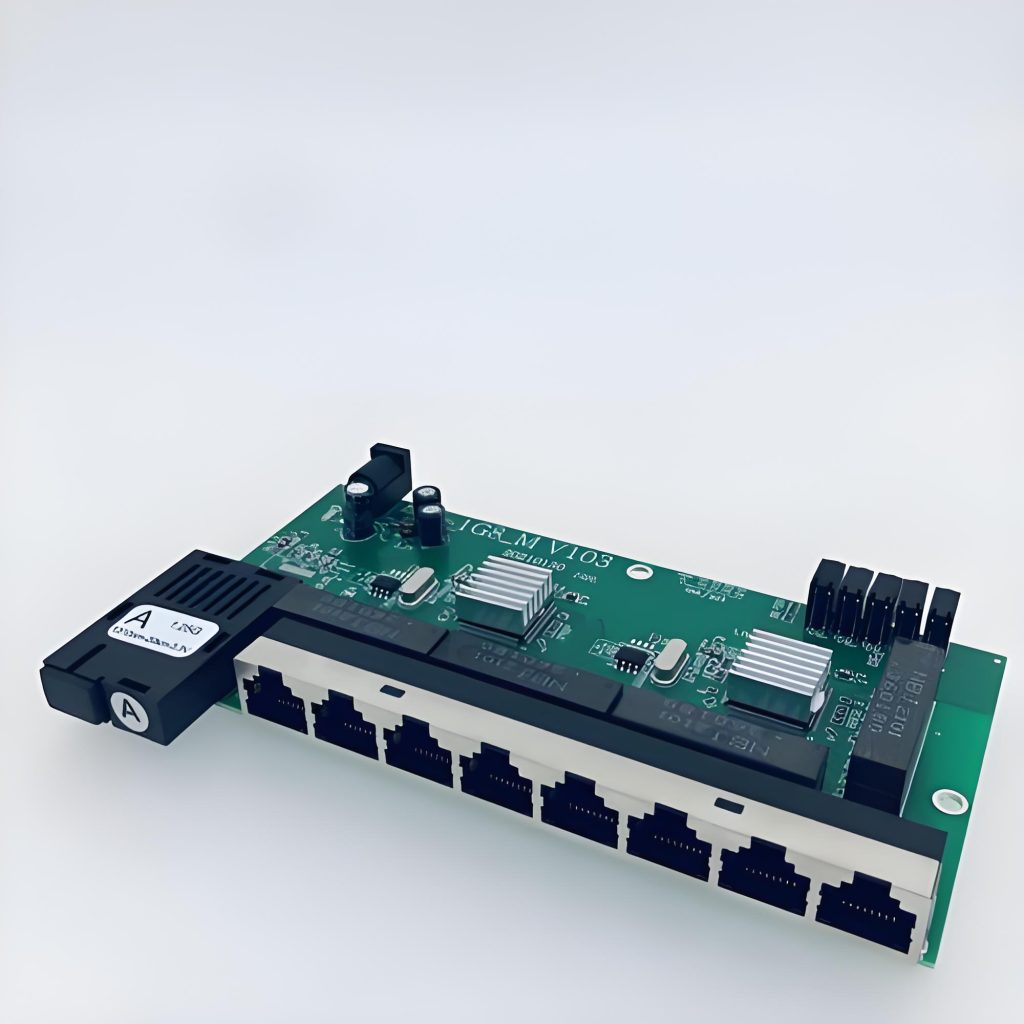
- Router and switch PCBs
- Communication modules and IoT devices
- Bluetooth / Wi-Fi module carrier boards
Industrial Controls
- PLC programmable logic controllers
- Power management modules
- Instrumentation circuit boards
- Motor drive control boards
Automotive Electronics (Non-Safety-Critical)
- In-vehicle infotainment systems
- Body control modules
- Sensor interface boards
Quality Assurance and Standards Compliance
Applicable Standards
UGPCB’s OSP antioxidant PCB product strictly follows these international standards:
| Standard | Title | Scope |
|---|---|---|
| IPC-4555 | Performance Specification for High Temperature Organic Solderability Preservatives (OSP) for Printed Boards | OSP process requirements and testing |
| IPC-6012E | Qualification and Performance Specification for Rigid Printed Boards | Finished board quality and performance |
| IPC-4101/21 | Specification for Glass-Reinforced Epoxy Laminate | FR-4 substrate technical requirements |
| IPC-TM-650 | Test Methods Manual | Various performance test methods |
| UL 94 V-0 | Flammability of Plastic Materials | Substrate flame retardant safety |
| RoHS 2.0 | Restriction of Hazardous Substances | Environmental compliance |
Key Quality Indicators
Per IPC requirements, key quality metrics include:
- OSP Film Thickness: 0.2–0.5μm, uniformity tolerance ≤ ±0.1μm
- Adhesion: ≥4B (IPC-TM-650 2.4.29 cross-cut test)
- Solder Spread Ratio: ≥80% (IPC-TM-650 2.4.1)
- Oxidation Protection Period: ≥6 months (ambient conditions)
- Flammability Rating: UL 94 V-0
Why Choose UGPCB for OSP Antioxidant PCBs?
Precision Manufacturing Capabilities
- 0.15mm minimum trace width / 0.20mm minimum spacing
- 0.45mm minimum finished hole size
- 1.6mm standard board thickness with excellent compatibility
Reliable OSP Process Control
- Strict adherence to IPC-4555 for film thickness and quality
- Full traceability throughout the manufacturing process
- Solderability testing and film thickness sampling for every batch
Fast Delivery
- Standard lead time: 7–10 working days
- Supports both prototype sampling and volume production
Comprehensive Technical Support
- Free DFM design review
- Professional engineering team for product selection guidance
Get a Quote Today
UGPCB delivers high-value OSP antioxidant PCB circuit board solutions. Whether you need prototype sampling or volume production, we provide professional technical support and competitive pricing.
📞 How to Get a Quote:
- Submit your Gerber files and BOM list
- Our engineering team responds with a customized solution and quote within 24 hours
- Free DFM check to ensure your design passes the first time
Data Source Statement: The technical data and standard requirements cited in this document are primarily derived from IPC (Association Connecting Electronics Industries) standards including IPC-4555 “Performance Specification for High Temperature Organic Solderability Preservatives (OSP) for Printed Boards,” IPC-6012E “Qualification and Performance Specification for Rigid Printed Boards,” IPC-4101/21 “Specification for Glass-Reinforced Epoxy Laminate,” IPC-TM-650 “Test Methods Manual,” and UL 94 “Standard for Tests for Flammability of Plastic Materials for Parts in Devices and Appliances.” Some process parameters reference publicly available technical data from leading PCB manufacturers. All data has been verified for accuracy.













