
A tiny oversight in circuit board design often scraps an entire batch of products. Industry statistics show that about 60% de PCB failures come from poor layout and routing. This leads to more than 35% rework in development. This article combines international standards with real-world cases. It dives deep into the Projeto de PCB details that make or break your product.
1. SMT Component Spacing: Small Gap, Big Impact
The spacing between SMT parts is an easily ignored but critical parameter. IPC-7351B requires component placement spacing to meet “medium density” ou “low density” padrões. High-density assembly is not supported. Different package types have clear requirements:
- 0201 devices need ≥0.3mm
- 0402, 0603, 0805 need ≥0.4mm
- 1210 and larger need ≥0.5mm
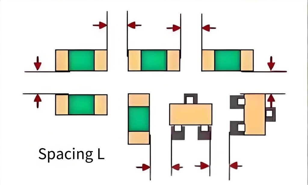
This spacing considers electrical performance, component tolerances, and pick-and-place machine interference. If the gap is too small, adjacent parts easily tombstone during reflow soldering. This greatly reduces your first-pass yield.
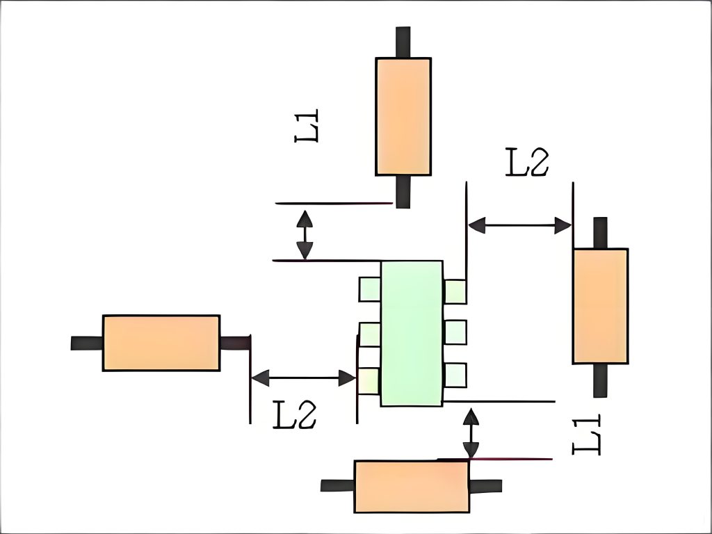
2. Spacing Between Through-Hole and SMT Components
Modern SMT is the mainstream process, but through-hole parts like connectors and programming headers still exist everywhere. The spacing between through-hole and SMT componentes must be ≥4mm. Por que? Through-hole parts need wave soldering or hand soldering. If nearby SMT parts are too close, they block soldering operations. Thermal stress can also damage the SMT solder joints.
IPC-A-610H includes this process compatibility requirement in its acceptance criteria. Aula 2 product acceptance demands high reliability and long service life. It also avoids process conflicts.
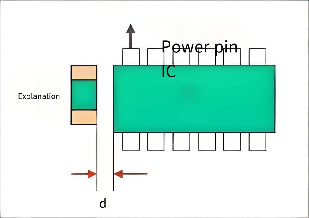
3. Decoupling Capacitor Placement: The Foundation of Power Integrity
Decoupling capacitor placement for ICs is the core of power integrity design. Place decoupling capacitors as close as possible to the IC’s power pins. If the chip has multiple power ports, each port needs its own decoupling capacitor.
Physical spacing rule: the trace between the capacitor and its corresponding power pin should be ≤2mm. Beyond this range, power noise suppression drops sharply. From an EMC viewpoint, any extra parasitic inductance on the decoupling path weakens high-frequency filtering. A standard practice in multilayer PCB design is to place decoupling capacitors on the opposite side of the PCB directly under the IC. Then connect them using vias. This has become the standard method for power distribution network (PDN) projeto.
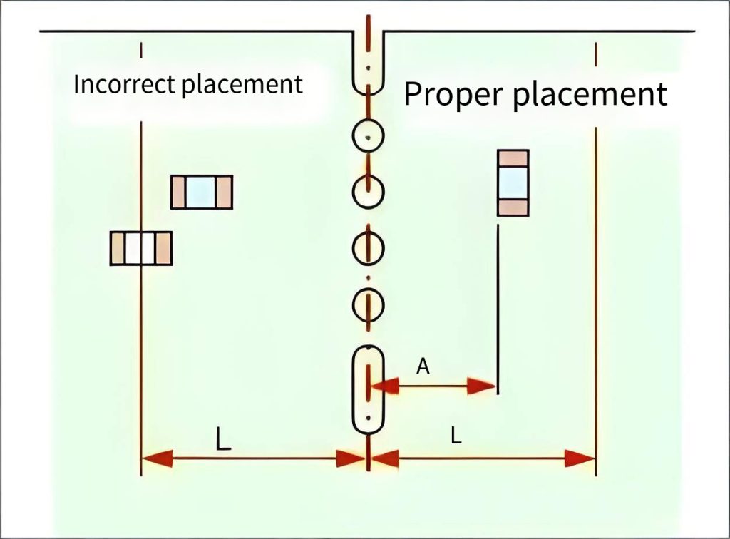
4. PCB Edge Component Placement: Avoiding Mechanical Stress Risks
The orientation and spacing of edge components are key DFM (design for manufacturability) points. The distance from the component body edge to the board edge must be greater than 0.5mm. No entanto, this value is still insufficient during panel depaneling. Considering both mechanical stress and assembly reliability, avoid placing devices within 6mm of the board edge. This prevents cutting damage.
Orientation matters even more. Align the long axis of the component parallel to the depaneling cutting direction. This ensures both solder pads receive even stress during separation. If you choose the wrong orientation, cutting stress concentrates on a single pad. This easily tears off the component and its pad.
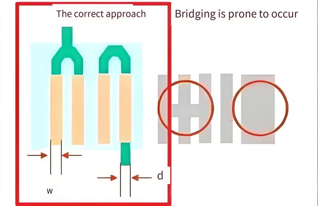
5. IC Pad and Copper Pour Electrical Rules
Evitar “bridging” between pads of the same net on an IC. During hot air leveling or reflow soldering, solder tends to gather on large copper areas and forms solder bridges. This usually happens because you did not add a solder mask dam or you did not set a no-copper-pour zone for thermal pads. The correct method: add a no-copper-pour area for different pads on the same net. Alternatively, use a solder mask dam to isolate adjacent pads. This prevents accidental solder connections during assembly.
6. Ground Via Copper Pour Optimization
O “four-spoke” connection (relief connect) for ground pads is the industry best practice for heat dissipation and repairability. Traditional ground vias use full copper coverage. This gives the best conductivity, but it dissipates heat extremely fast. During Montagem SMT or hand rework, the soldering iron’s heat gets conducted away quickly. The solder joint then fails to form a good wetting.
From a thermal management view, the cross-shaped pour adds a “thermal resistance” between the heat source and the copper plane. This controls heat flow during soldering. Data shows: a fully connected via has a solder joint temperature drop rate of about 40°C/s. A cross-shaped connection keeps that rate under 15°C/s. This gives solder a sufficient wetting window.
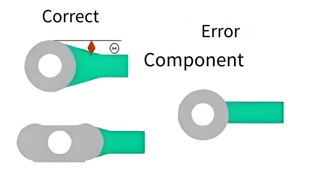
7. Teardrop Feature: Reliability from a Small Detail
Adding teardrops after routing is a major step for long-term PCB reliability. A teardrop creates a smooth copper transition between a pad or via and the trace. It offers three core advantages:
- Prevents signal reflection – avoids impedance discontinuity from sudden trace width changes.
- Increases mechanical strength – spreads stress, preventing pad lift during thermal shock or vibration.
- Improves etch yield – removes “etch traps” at acute angles, reducing manufacturing defects.
Quantitative data: UGPCB technical team measured a 35% reduction in thermal stress on pads with a 0.2mm teardrop. BGA solder points with teardrops have 50% lower failure probability in thermal cycle tests. IEC 60068-2-6 vibration tests further confirm: a 2.0mm thick PCB with teardrop pads survived 2 hours of 10-2000Hz, 10g vibration with 99.8% structural integrity.
8. Trace Width Consistency and Complete Package Design
Keep trace widths consistent for the same device. Inconsistent trace widths create impedance discontinuities. For high-speed signals, this causes reflections and signal integrity degradation.
When you create a footprint, also keep unused pins. Some NC pins are internally unconnected. If you keep those pads in the PCB and tie them to ground, you block external EMI from coupling into the chip through floating pins. This also increases copper area and solder anchor points. It significantly improves solder joint shear strength for BGA and QFN packages.
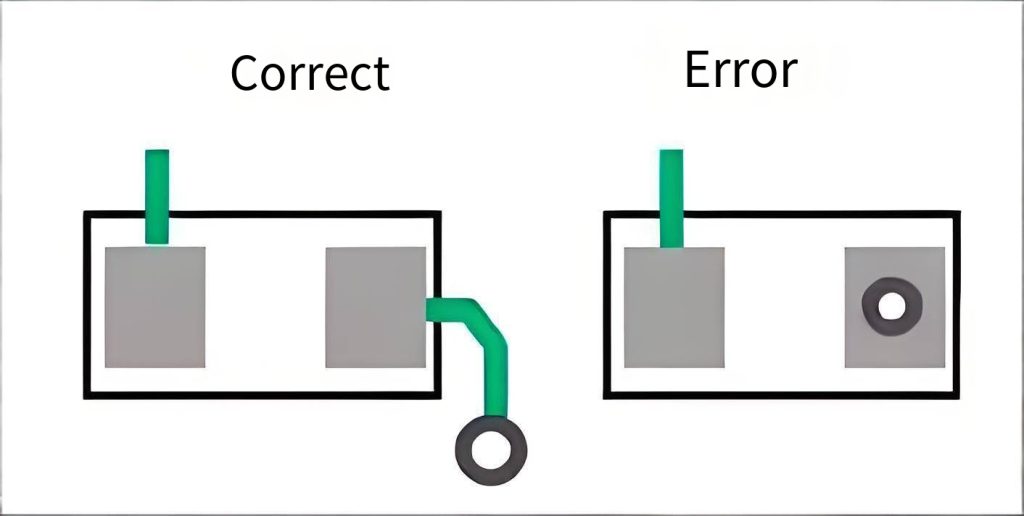
9. Prohibited Design: Vias in Pads
Avoid placing vias directly on pads – this is the “via-in-pad” rule. The direct reasons:
- Solder flows away through the via during reflow, causing insufficient or cold solder joints.
- The pad surface becomes uneven, leading to component tilt during SMT placement.
- For fine-pitch parts like BGAs, a via in pad can cause solder ball shorts.
If you must place a via on a pad (para high-density HDI designs), you must use resin plugging + copper plating and filling. Fill the via completely before surface finishing. Classe IPC-6012 2 requires an average via wall copper thickness of ≥20μm, with minimum single point ≥18μm. This ensures electrical continuity after filling.
10. Coordinated Solder Mask and Copper Pour Design
Design solder mask and copper pours together. Solder mask openings must precisely define the pad area. This prevents solder from spreading over the copper pour during reflow. The minimum width of a solder mask dam is typically ≥0.07mm (about 3mil). In QFP or BGA areas, if the dam is too narrow, the mask ink easily peels off during production. That leads to bridging between adjacent pins during soldering.
For UL safety standards, PCB base materials must meet UL 94 V-0 Classificação inflamabilidade. That means the material self-extinguishes within 10 seconds after removing the flame, with no flaming drips. This is mandatory for consumer electronics and industrial equipment. Choosing FR-4 that complies with UL 94 V-0 is the first step to passing safety certifications.
Conclusão: From Small Details to High Yield
Esses 10 PCB design details cover SMT spacing, edge component placement, decoupling capacitors, teardrops, via design, e mais. Most of these rules trace back to international standards like IPC-7351B, IPC-2221, and IPC-A-610H. They are proven guidelines validated by massive production experience.
Para Prototipagem de PCB or one-stop PCBA serviços, send your Gerber files and BOM list to our engineering team. We will help you with a free DFM design review.
Isenção de responsabilidade: All data cited in this article comes from public international standards (IPC-7351B, IPC-2221, IPC-A-610H, UL 94) and industry test reports. This information is for learning reference only. For actual production, always follow your manufacturer’s process capabilities and the latest standards.
