
PCB HDI de 8 camadas 1 + N + 1 da UGPCB: A Comprehensive Guide
In the relentless pursuit of miniaturization and enhanced performance in electronics, Interconexão de alta densidade (IDH) PCB have become the cornerstone. UGPCB’s 8-Layer 1+N+1 HDI product represents a sophisticated solution for designers pushing the boundaries of what’s possible. This article provides a detailed look at this advanced placa de circuito impresso tecnologia.
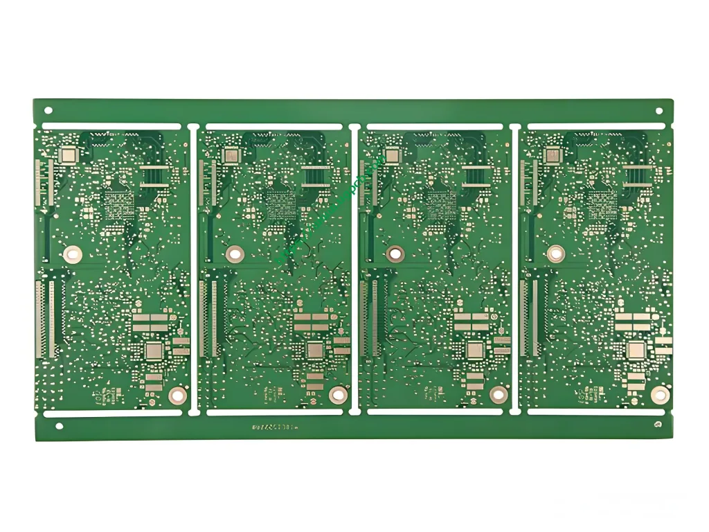
What is an 8-Layer 1+N+1 HDI PCB?
An 8-Layer 1+N+1 HDI PCB is a specific type of high-density interconnect board. The nomenclature “1+N+1” describes its microvia build-up structure.
-
The First and Last ‘1’: These represent a single layer of high-density microvias on the top and bottom surfaces of the board. These microvias are typically created using laser drilling.
-
The ‘N’: This represents the core of the board, which in this case is a standard 6-layer PCB multicamadas (making the total 8 camadas). The core contains through-holes or buried vias that connect the internal layers.
This structure allows for a very high number of interconnections in a compact space, making it ideal for complex, space-constrained Designs de PCB essential for modern microelectronic products.
Key Design Features and Specifications
UGPCB manufactures this HDI PCB with precision, adhering to the following critical specifications:
-
Material: High-Tg FR-4, a robust and reliable laminate offering excellent thermal and mechanical stability.
-
Espessura da placa: A finished thickness of 0.8mm, supporting slim product profiles.
-
Copper Weight: 1 onças (35µm) for inner layers and 0.5 onças (17.5µm) para camadas externas. This balance ensures good current carrying capacity while allowing for finer outer layer trace etching.
-
Acabamento superficial: Imersão Ouro (CONCORDAR) over an OSP (Conservador de solda orgânica) foundation. This combination provides a flat, durable surface for soldering and excellent shelf life.
-
Rastreio/espaço mínimo: 3 mil (0.075 milímetros), enabling high-density circuitry.
-
Tamanho mínimo do orifício: 0.2mm for mechanical drills and an ultra-fine 0.1mm for laser-drilled microvias.
How This HDI PCB Structure Works
O “1+N+1” architecture functions by creating a more efficient routing pathway. Instead of using large through-holes that consume valuable real estate on every layer, this HDI PCB design utilizes microvias. These tiny laser-drilled holes connect only adjacent layers (por exemplo, L1 to L2, or L8 to L7). Esse “stacked” ou “staggered” via approach frees up routing channels on the inner layers, allowing for a much greater component density and more efficient signal paths, which is crucial for high-speed Montagem PCBA.
Primary Applications and Use Cases
The primary application for this advanced HDI PCB is in sophisticated microelectronic products. Specific use cases include:
-
Tecnologia vestível: Smartwatches, fitness trackers, and medical monitors.
-
Advanced Mobile Devices: Smartphones, comprimidos, and ultra-portable laptops.
-
High-Density Medical Equipment: Miniaturized medical imaging and diagnostic devices.
-
Aerospace and Defense Avionics: Where reliability and size are paramount.
The Material Composition: FR-4 Laminate
The choice of FR-4 material is strategic. It provides an excellent balance of performance, custo, and manufacturability. For this 0.8mm thick HDI PCB, a high-grade FR-4 with a high glass transition temperature (Tg) is used to withstand the thermal stress of multiple lamination cycles and lead-free PCBA soldering processes.
Performance and Structural Advantages
The structure of the 1+N+1 HDI board directly translates to significant performance benefits:
-
Enhanced Signal Integrity: Shorter interconnection paths reduce signal loss and propagation delay.
-
Improved Thermal Management: The dense via structure aids in heat dissipation.
-
Superior Reliability: The use of microvias reduces the risk of solder joint failure during thermal cycling.
-
Reduced Size and Weight: The core advantage of HDI technology, enabling smaller end products.
A Simplified Overview of the Production Process
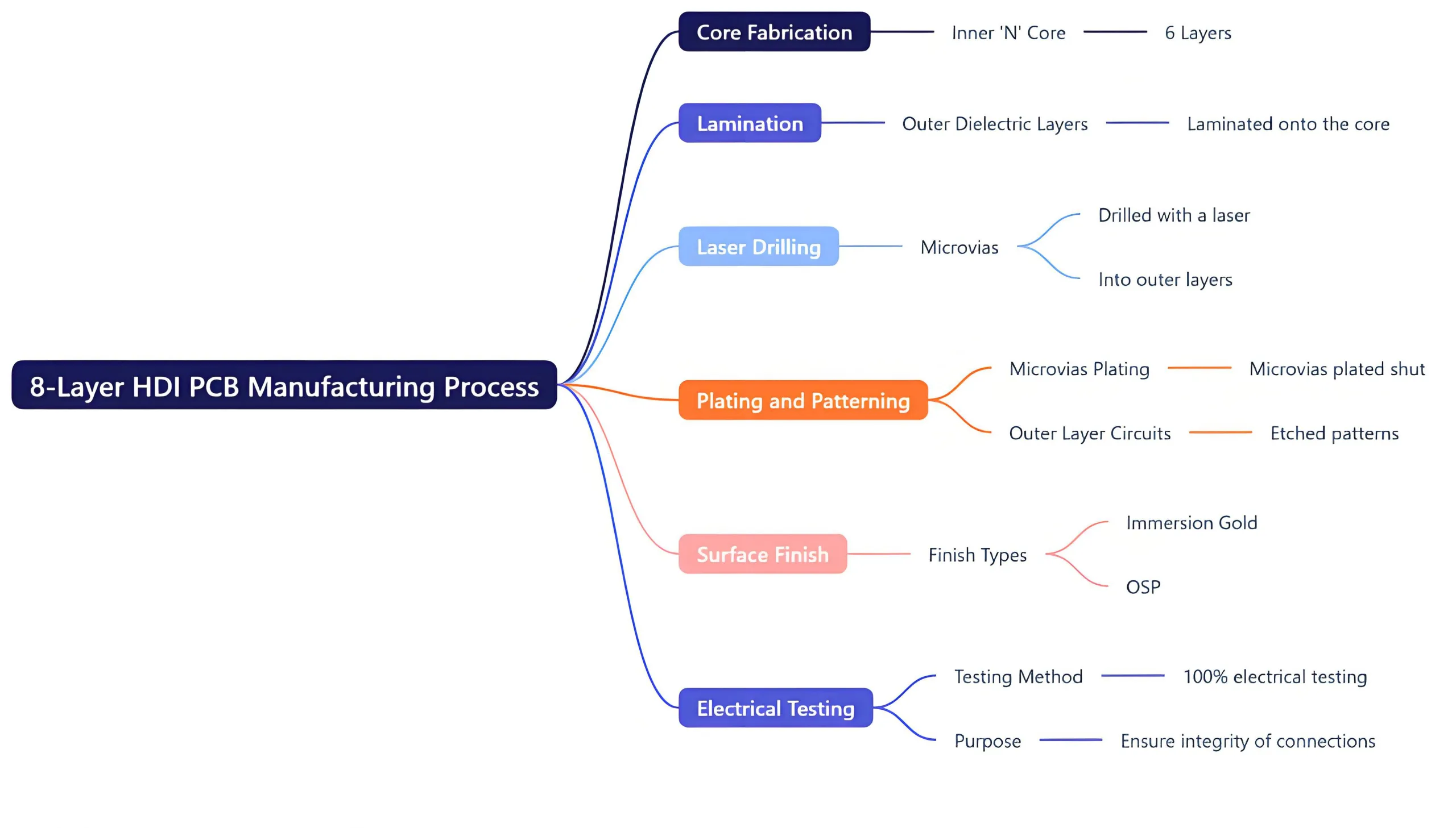
The manufacturing of this HDI PCB is a multi-step, precision process:
-
Core Fabrication: The inner ‘N’ essencial (6 camadas) is produced first.
-
Laminação: Outer dielectric layers are laminated onto the core.
-
Perfuração a laser: Microvias are drilled with a laser into the outer layers.
-
Plating and Patterning: The microvias are plated shut, and the outer layer circuits are etched.
-
Acabamento superficial: The Immersion Gold and OSP are applied.
-
Teste elétrico: 100% electrical testing ensures the integrity of all connections.
Why Choose UGPCB for Your HDI PCB and PCBA Needs?
UGPCB’s expertise in manufacturing 8-Layer HDI PCBs offers distinct advantages for your project. Their capability to reliably produce boards with 3/3 mil lines and 0.1mm microvias positions them as a leader for complex PCB manufacturing. This makes them an ideal partner not just for Fabricação de PCB but also for a full turnkey PCBA service, ensuring a seamless transition from design to a finished, assembled product.


