
UGPCB's 2 Layers GPS Module PCB: Reliable Precision for Modern Applications
Welcome to UGPCB, where we specialize in high-quality PCB e PCBA soluções. Nosso 2 Layers GPS Module PCB is engineered for accuracy and durability, making it an ideal choice for various GPS-based systems. Designed with industry standards like IPC-6012, this product ensures superior performance in demanding environments. Whether you’re developing navigation devices or IoT trackers, this PCB delivers the reliability you need. Read on to discover how our GPS Module PCB can elevate your projects and drive innovation.
Overview of the 2 Layers GPS Module PCB
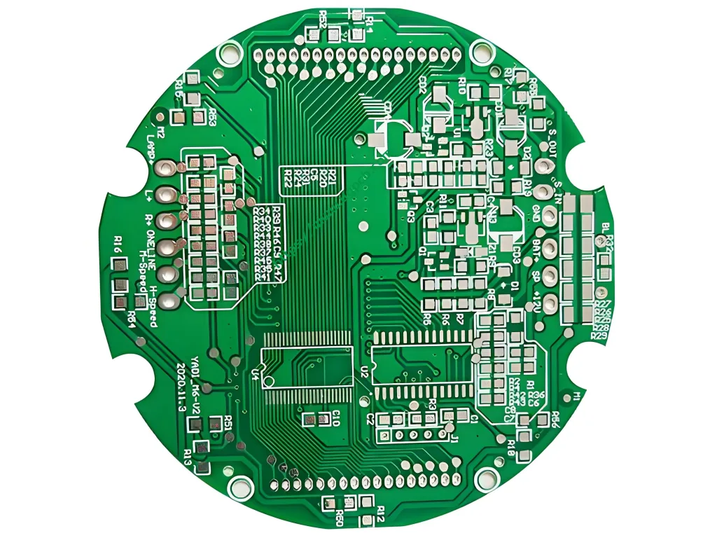
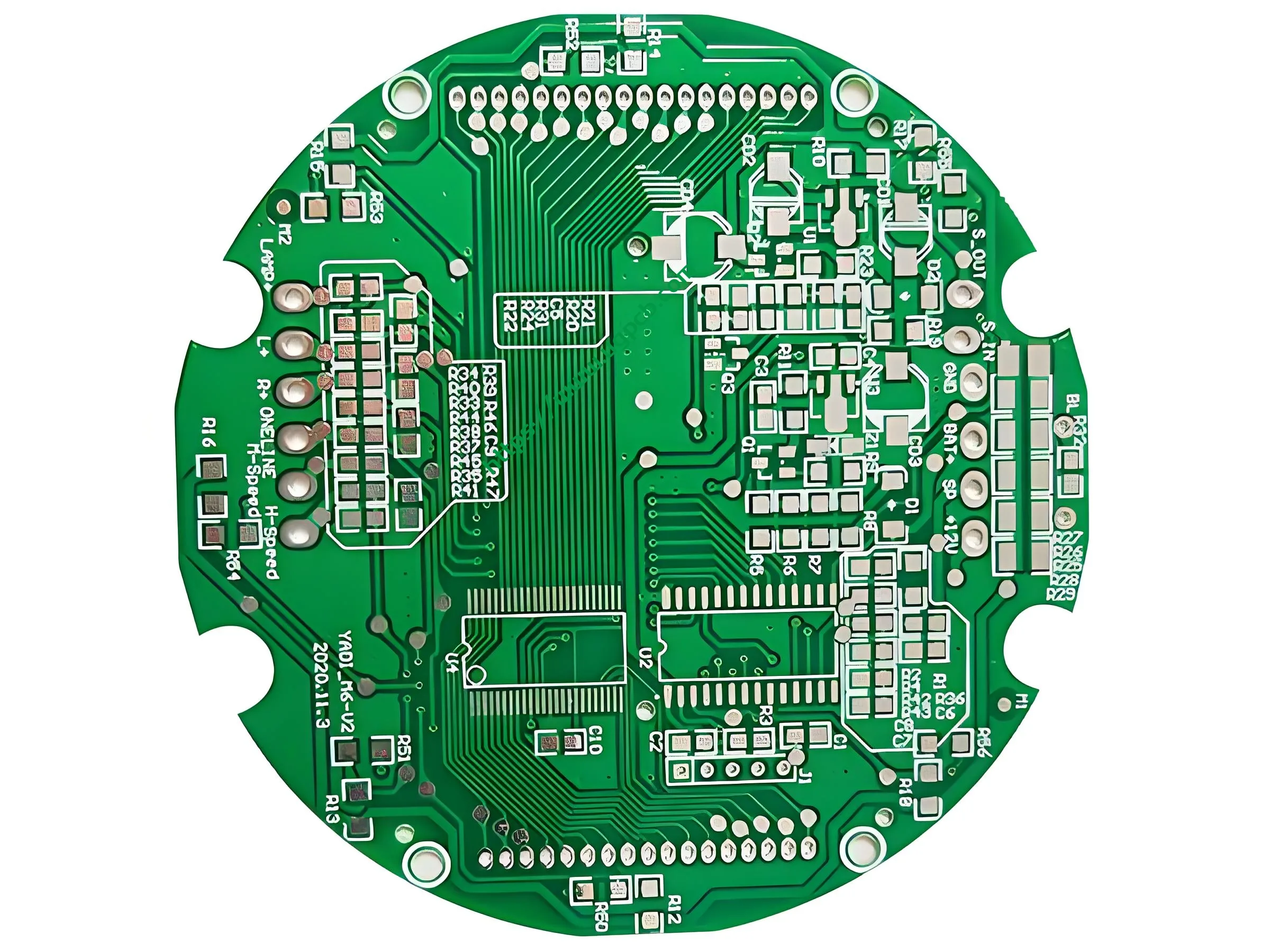
O 2 Layers GPS Module PCB is a compact, double-sided placa de circuito impresso specifically designed for GPS applications. It serves as the core component in devices that require precise location tracking, offering excellent signal integrity and thermal stability. With parameters such as 1.0mm finished thickness and 4mil trace/space, this PCB is optimized for high-frequency operations, making it a top choice for Fabricantes de PCBA and engineers seeking efficient GPS solutions.
What Is a GPS Module PCB?
A GPS Module PCB is a specialized circuit board that integrates GPS receivers and related components to process satellite signals for location data. UGPCB’s 2-layer version uses a simple yet effective design, with two conductive layers separated by an FR4 dielectric core. This structure supports essential functions like signal amplification and data transmission, ensuring seamless integration into broader PCBA assemblies for applications ranging from automotive to consumer electronics.
Design Key Points for Optimal Performance
When designing this GPS Module PCB, key considerations include impedance control, Gerenciamento térmico, e integridade do sinal. The 4mil trace/space allows for dense routing, while the 1OZ copper thickness ensures adequate current carrying capacity. Immersion gold surface treatment enhances solderability and corrosion resistance, critical for long-term reliability in PCBA processes. Adhering to IPC-2221 standards, our design minimizes electromagnetic interference and maximizes efficiency in GPS signal reception.
How the GPS Module PCB Works
This PCB operates by receiving signals from GPS satellites through embedded antennas and processing them via integrated circuits. The two-layer design facilitates efficient power distribution and signal routing, with the FR4 material providing insulation to prevent short circuits. As part of a PCBA, it converts raw data into usable coordinates, enabling real-time tracking and navigation in devices like smartwatches or fleet management systems.
Common Applications of the GPS Module PCB
O 2 Layers GPS Module PCB is versatile and finds use in numerous fields, including automotive navigation, wearable technology, asset tracking, and drones. Its robust construction makes it suitable for harsh environments, such as outdoor adventures or industrial monitoring. By incorporating this PCB into your PCBA, you can develop innovative products that rely on accurate GPS functionality, from logistics solutions to personal safety devices.

Classification of GPS Module PCBs
GPS Module PCBs can be categorized based on layer count, material, and application. UGPCB’s model falls under the 2-layer rigid PCB classification, using FR4 material for general-purpose use. Other types include flexible or PCB multicamadas for advanced needs, but this 2-layer version offers a cost-effective solution for standard GPS PCBA requirements, balancing performance and affordability.
Materials Used in Construction
The primary material is FR4, a flame-retardant epoxy laminate known for its mechanical strength and electrical insulation. The copper layers are 1OZ thick, providing reliable conductivity, while the immersion gold finish on the surface ensures excellent connectivity and durability. This material selection complies with IPC-4101 standards, guaranteeing that the PCB withstands environmental stressors in various PCBA applications.
Características de desempenho
This GPS Module PCB excels in performance with low signal loss, high thermal resistance, and stable impedance. The 1.0mm thickness and 4mil trace/space contribute to minimal crosstalk, ensuring accurate GPS data processing. It operates efficiently across a wide temperature range, making it ideal for PCBA in automotive or outdoor devices where reliability is paramount.
Detalhes estruturais
Estruturalmente, the PCB consists of two copper layers laminated onto an FR4 substrate, with a solder mask in green or white for protection. Vias connect the layers, enabling complex routing for GPS componentes. The immersion gold surface treatment provides a flat, reliable interface for component mounting during PCBA, enhancing overall assembly quality and longevity.
Key Features of the 2 Layers GPS Module PCB
-
Alta precisão: 4mil trace/space allows for detailed layouts, improving signal accuracy in GPS applications.
-
Durabilidade: FR4 material and immersion gold treatment offer resistance to moisture and wear.
-
Ease of Integration: Designed for straightforward PCBA processes, reducing assembly time and costs.
-
Versatilidade: Suitable for a wide range of GPS devices, from consumer gadgets to industrial tools.
-
Conformidade: Atende Padrões IPC, ensuring consistency and reliability in mass production.
Production Process at UGPCB
Our production follows a streamlined workflow: design validation, material preparation, layer lamination, perfuração, revestimento, gravura, aplicação de máscara de solda, tratamento de superfície (ouro de imersão), e testes. Each step adheres to IPC-A-600 guidelines, with quality checks to ensure the PCB meets specifications for PCBA integration. This process guarantees that every 2 Layers GPS Module PCB delivers optimal performance and reliability.
Typical Usage Scenarios
This PCB is commonly used in scenarios such as vehicle tracking systems, personal navigation devices, sports wearables, and agricultural monitoring equipment. Its ability to handle high-frequency signals makes it perfect for real-time location-based services in PCBA setups, enabling innovations in smart cities and IoT ecosystems.
Conclusão: Elevate Your Projects with UGPCB’s GPS Module PCB
UGPCB's 2 Layers GPS Module PCB combines advanced design, reliable materials, and proven performance to meet your GPS and PCBA needs. Whether you’re prototyping or scaling production, this product offers the precision and durability required for success. Visit our website to learn more or request a quote today—let’s build the future of navigation together!


