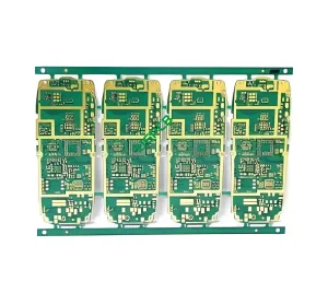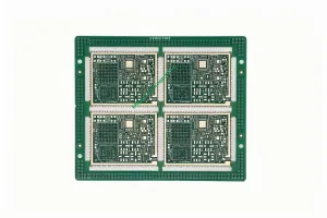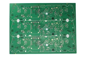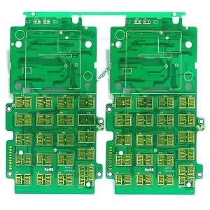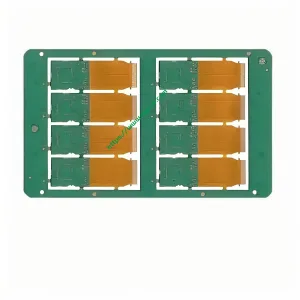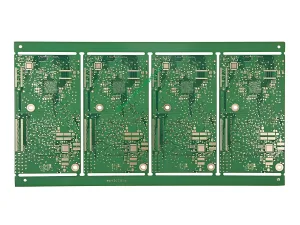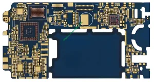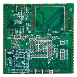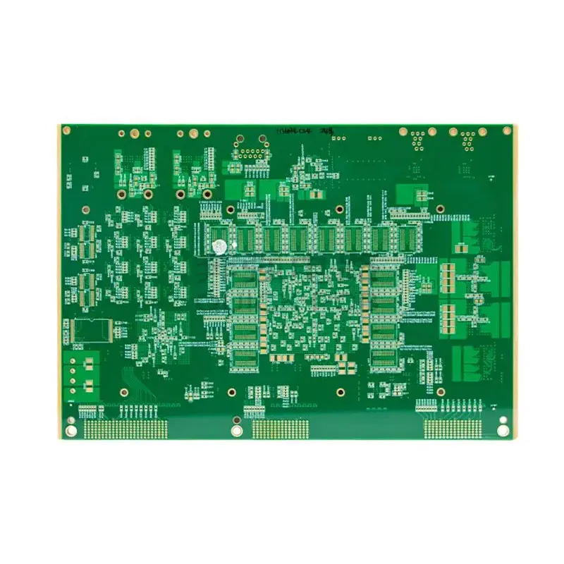
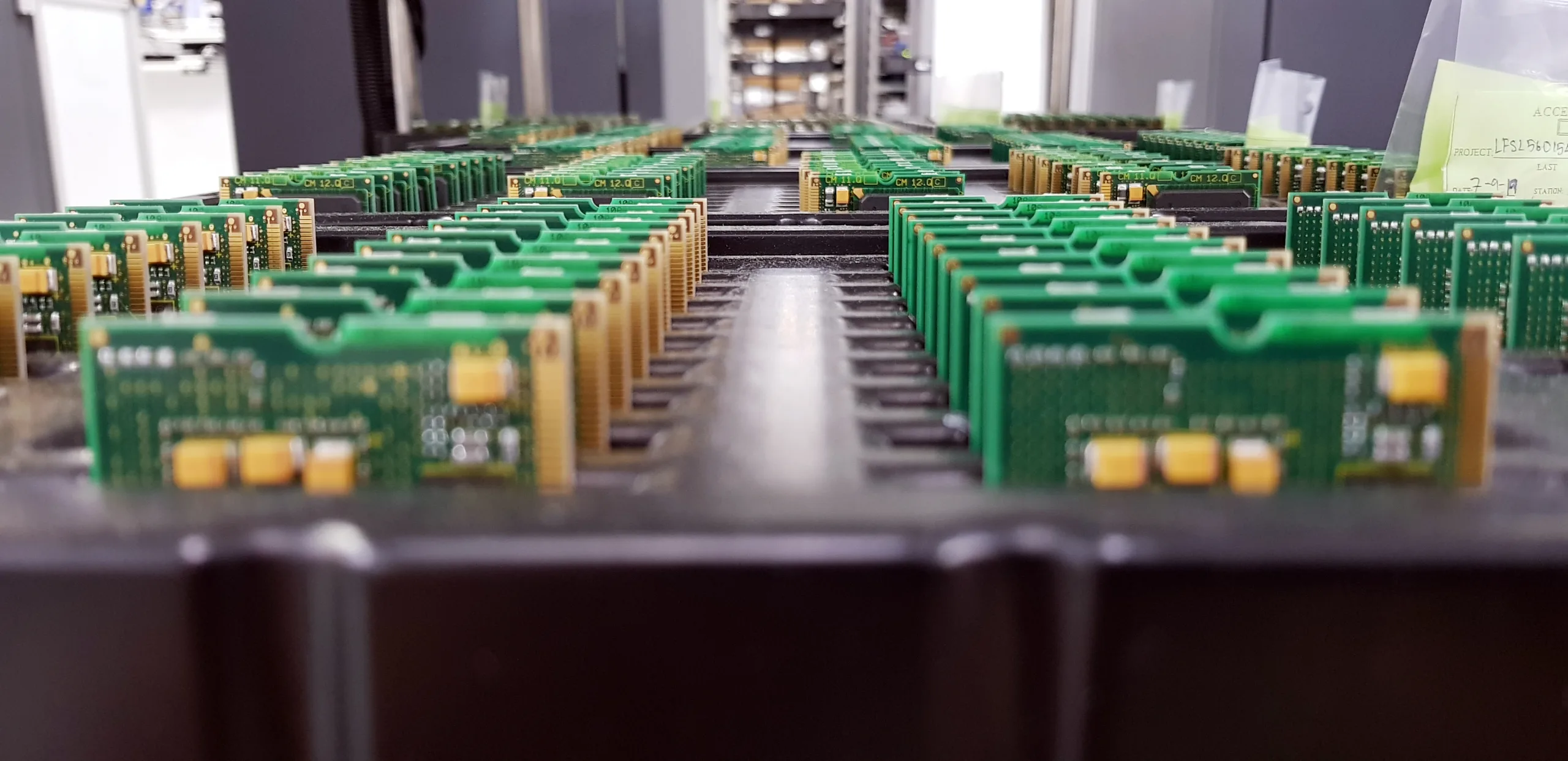
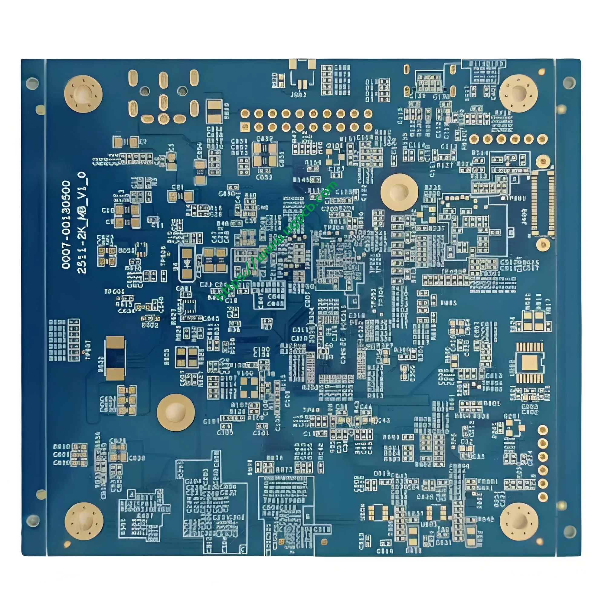


Product positioning: UGPCB’s 6-layer 1-stage HDI PCB uses a 1+N+1 stack-up. Ele oferece 0.10 mm laser blind vias, 0.20 mm through holes, 0.20 mm BGA pitch, e 3/3 mil traces. It suits compact, high-integration electronics.
1. What Is a 6-Layer 1-Stage HDI PCB?
A 6-layer 1-stage HDI PCB is a six-layer high-density interconnect printed circuit board. It uses a 1+N+1 stack-up, where N equals 4. IPC-2226 classifies this build-up approach as a Type I IDH estrutura. Each side has one build-up layer. Laser microvias connect the outer layers to the next inner layer. Mechanical through holes connect the core layers.

Parameter Snapshot
| Parâmetro | Especificação |
|---|---|
| Contagem de camadas | 6 camadas (1+N+1) |
| Base material | FR4 Tg150 |
| Espessura da placa | 1.6 milímetros |
| Tamanho do painel | 105 × 95 milímetros (1-acima) |
| Espessura externa do cobre | 35 µm (1 onças) |
| Espessura interna do cobre | 30 µm |
| Furo passante mínimo | 0.20 milímetros |
| Minimum blind via | 0.10 milímetros |
| Minimum BGA pitch | 0.20 milímetros |
| Trace width/spacing | 3/3 mil (75 µm/75 µm) |
2. Product Overview and Scientific Classification
2.1 Visão geral do produto
UGPCB’s 6-layer 1-stage HDI PCB targets high-density electronic packaging. It improves routing density over a standard 6-layer through-hole PCB. Laser-drilled blind vias make this possible. IPC-2226 defines HDI as a board with higher wiring density than PCBs convencionais. It uses conductors ≤100 µm, vias <150 µm, and pads <400 µm. This product meets those thresholds. Isso é 3/3 mil (75 µm) traces and 0.10 mm laser microvias exceed standard PCB capability.
2.2 Classificação Científica
- By interconnection: PCB HDI, IPC-2226 Type I
- By stack-up: 1+N+1 first-order HDI, single build-up per side, N=4 core
- Por contagem de camadas: 6-camada PCB multicamadas
- By base material: FR4 Tg150 epoxy glass fabric
- By performance class: Classe IPC-6012 2 or Class 3
- By product form: bare PCB or Montagem PCBA
3. Stack-Up and Design Highlights
3.1 1+N+1 Stack-Up
1+N+1 is the most basic and mature HDI stack-up. “N” is the core. Each “1” is one build-up layer. This product is 1+4+1. The core has four layers. One build-up layer sits on each side. IPC-2226 describes this structure as having microvias that connect to adjacent inner layers. The core uses mechanical through holes. This structure balances signal integrity, custo, and yield. Many HDI PCB designs start with this stack-up.

3.2 Key Design Points
Blind via design: The minimum blind via is 0.10 milímetros (100 µm). IPC-T-50M defines a microvia as a blind via ≤0.15 mm with aspect ratio ≤1:1. The blind via connects only the outer layer to the next inner layer. It frees inner-layer routing space. This helps high-density PCB layout.
Trace width and spacing: The product uses 3/3 mil (75 µm/75 µm) vestígios. This is a core PCB HDI capacidade. Standard multilayer PCBs often use 6/6 mil (150 µm) vestígios. HDI PCBs can use 3/3 mil or finer. This doubles routing density in the same area. No 0.20 mm BGA pitch, 3/3 mil traces allow two routes between pads. This directly affects BGA escape routing.
BGA support: The minimum BGA pitch is 0.20 milímetros. At this pitch, pads are often 0.10–0.12 mm. Pad spacing is only 0.08–0.10 mm. This demands high registration accuracy and etch control in PCB manufacturing.
Controle de impedância: Com 3/3 mil traces and FR4 Tg150, Dk is about 4.2–4.6 at 1 MHz. Manufacturers can control 50 Ω single-ended and 100 Ω differential impedance. This supports high-speed signal transmission.
Thermal design: The 6-layer structure uses 30 µm inner copper. Large inner copper planes spread heat away from BGA areas.
4. Como funciona
The 6-layer 1-stage HDI PCB uses two via types:
- Laser blind via: A laser drills from the outer layer to the next inner layer. The minimum diameter is 0.10 milímetros. CO₂ or UV lasers form these vias.
- Mechanical through hole: This hole passes from top to bottom. It connects core layers and all layers. The minimum diameter is 0.20 milímetros.
Signals travel from surface components, such as BGA chips, through blind vias into inner signal layers. This avoids the space loss and signal reflection of through holes. The shorter path lowers parasitic inductance and capacitance. This benefits high-speed digital signals.
5. Core Materials and Performance
5.1 Material base: FR4 Tg150
This product uses FR4 Tg150 epoxy glass fabric. Tg is the glass transition temperature. IPC-TM-650 method 2.4.25 (DSC) measures this value. Tg150 material remains stable in lead-free soldering. Lead-free reflow peaks at about 245–260°C. The material withstands multiple reflow cycles without major dimensional change or delamination.
5.2 Espessura do Cobre
- Outer copper: 35 µm (1 onças). This supports current carrying and solder reliability.
- Cobre interno: 30 µm. This meets signal and power plane needs.
5.3 Key Performance Features
- High routing density: 3/3 mil traces and 0.10 mm microvias raise density by over 50% versus standard 6-layer boards.
- Small package support: 0.20 mm BGA pitch fits CSP, QFN, and other micro packages.
- Strong signal integrity: Short blind via paths reduce parasitic effects. This helps high-speed signals.
- Reliable construction: The board can meet IPC-6012 acceptance requirements. Classe IPC-6012 3 requires a minimum average copper thickness of 25 µm in plated holes.
6. Processo de Produção
UGPCB makes 6-layer 1-stage HDI PCBs through precise steps:
- Inner-layer imaging: Expose, desenvolver, and etch inner traces on the 4-layer core.
- Inner-layer lamination: Press inner cores and prepreg into a 4-layer core.
- First drilling and plating: Drill mechanical through holes and plate copper.
- Build-up lamination: Press one dielectric layer on each side of the core.
- Perfuração a laser: Use CO₂ or UV lasers to form 0.10 MM Microvia.
- Blind via plating and filling: Plate and fill laser vias for reliable conduction.
- Outer-layer imaging: Form 3/3 mil outer traces.
- Máscara de solda e acabamento superficial: Apply solder mask and ENIG or OSP finish.
- Profiling and testing: Route the outline, run teste de sonda voadora, AOI, and final inspection.
7. Principais aplicações
The 6-layer 1-stage HDI PCB balances density, tamanho, e confiabilidade. It serves many markets:
- Smartphones and mobile devices: Mainboard core areas with processor BGA packages.
- Vestíveis: Relógios inteligentes, TWS earbuds, and other space-limited products.
- Eletrônica automotiva: ADAS sensor modules and infotainment mainboards.
- Medical electronics: Portable monitors and implantable device control boards.
- Controle industrial: PLC modules and industrial IoT gateways.
- Equipamento de comunicação: 5G small-cell RF modules and optical module PCBs.

The global HDI PCB market is growing fast. The Business Research Company reports strong HDI market growth. The market will grow from USD 17.78 bilhão em 2025 to USD 19.47 bilhão em 2026. That is a 9.5% compound annual growth rate (Cagr). The market may reach USD 28.82 bilhão por 2030.
8. Por que escolher UGPCB?
UGPCB Circuitos Limitados (UGPCB®) focuses on high-precision PCB R&D and manufacturing. Its factory covers 280,000 metros quadrados. Emprega 1,300 pessoas. Sobre 35% are technical professionals. The company makes HDI PCBs from 1 para 6+ etapas, placas HDI de qualquer camada, Substratos IC, placas rígidas-flexíveis, e PCBs FR4 multicamadas padrão.
UGPCB holds ISO9001, UL, and RoHS certifications. It follows IPC standards for production and acceptance. This ensures product quality meets customer needs and industry rules. The company serves customers in mainland China, Taiwan, Coréia, Japão, the US, Brasil, Índia, Sudeste Asiático, and Europe.
Get a quote today: Send your Gerber files or design parameters. The UGPCB technical team will reply within 24 horas. We will provide a custom 6-layer HDI PCB quote and a one-stop PCBA assembly solution. Se você precisa quick prototyping or stable volume supply, we can help.
Declaração da fonte de dados
This article cites standards and technical data from these authorities:
- IPC-2226, Sectional Design Standard for High Density Interconnect (IDH) Quadros Impressos — HDI structure classification and microvia definition.
- IPC-T-50M, Terms and Definitions for Interconnecting and Packaging Electronic Circuits — microvia terminology.
- IPC-6012, Especificação de qualificação e desempenho para placas impressas rígidas — rigid board acceptance and plated copper thickness.
- IPC-2221, Padrão genérico para design de placas impressas — PCB design guidelines and trace/space practice.
- IPC-TM-650 Method 2.4.25 — glass transition temperature (Tg) test method.
- The Business Research Company, Global High Density Interconnect (IDH) Market Report 2026 — HDI market data.