
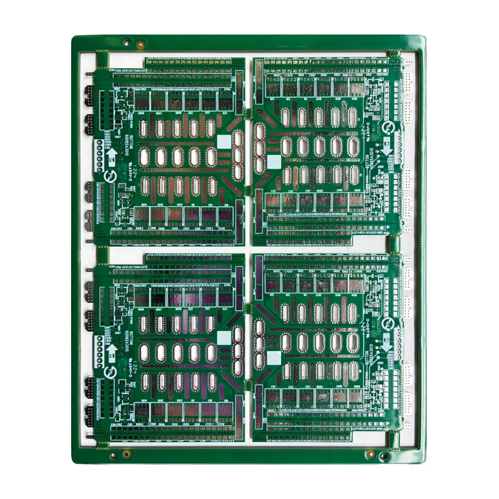
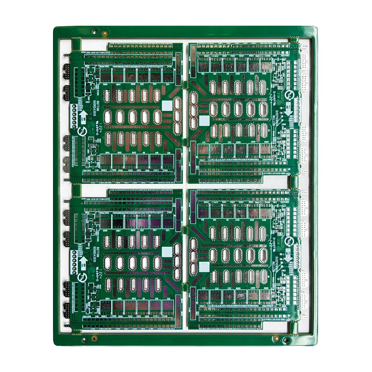
High-Reliability 8-Layer Rigid PCB Visão geral do produto & Definição
In the realm of high-speed, high-density electronic design, multilayer PCBs (Placas de circuito impresso) are indispensable. UGPCB's 8-layer rigid PCB, built with a substantial 2.0mm board thickness e 3OZ heavy copper foil, is engineered to withstand demanding electrical and physical environments. It serves not only as the foundation for electrical connectivity but as a critical component ensuring device stability and enhanced product reliability. For applications in industrial controls, power systems, or automotive electronics, this high-specification board is the optimal solution for complex, high-performance designs.
Especificações principais
-
Contagem de camadas: 8-Layer Rigid PCB
-
Finished Board Thickness: 2.0mm ±10%
-
Material base: FR-4, Temperatura de transição vítrea (Tg) ≥ 170°C
-
Acabamento superficial: Lead-Free Hot Air Solder Leveling (HASL-LF)
-
Peso de cobre: 3 ounces per square foot (≈105μm) for both inner and outer layers
-
Máscara de solda & Silkscreen: Green LPI Solder Mask, White Silkscreen Legend
Critical Design Considerations
When designing with this high-specification PCB, engineers must prioritize:
-
Gerenciamento térmico: Leverage the high current-carrying capacity of 3OZ heavy copper to optimize power and ground planes, reducing impedance and heat rise. Use thermal simulation in conjunction with the high heat resistance of FR-4 TG170 material.
-
Controle de impedância & Integridade do sinal: The 8-layer stack-up allows effective separation of signal, poder, e camadas terrestres. Precise calculation and control of trace impedance (por exemplo, 50Ω single-ended, 100Ω differential) is essential to minimize reflection and crosstalk.
-
Mecânico & Electrical Reliability: O 2.0mm thick board enhances overall rigidity, suitable for applications with vibration or insertion stress. For high-voltage or high-current nodes, adjust trace width and clearance according to IPC-2221 standards and the 3OZ copper weight to ensure safety margins.
-
Dfm (Design para fabricação): Collaborate with UGPCB’s engineering team early to address specific requirements for heavy copper PCB e thick board PCB processing, such as drilling parameters and plating uniformity, ensuring a high-yield manufacturing process.
How It Works & Estrutura
An 8-camada PCB is fabricated by laminating multiple conductive layers into a single unit using precise processes including inner-layer imaging, laminação, perfuração, and plating. Electrical connections between layers are established via plated through-holes (PThs), vias cegas, or buried vias. A typical stack-up example is:
Top Layer (Sinal) — Prepreg — L2 (Chão) — Core — L3 (Sinal) — Core — L4 (Poder) — Core — L5 (Sinal) — Prepreg — Bottom Layer (Sinal)
Esse “sandwich” structure effectively isolates high-speed signals, provides solid reference planes, and ensures efficient power distribution.
Desempenho & Key Features
-
Superior Electrical Performance: 3OZ heavy copper provides extremely low conductor resistance and excellent current-carrying capacity (over 3x that of standard 1OZ copper), reducing power loss and voltage drop.
-
Exceptional Thermal Reliability: FR-4 TG170 high Tg material withstands higher operating and soldering temperatures. Combined with the thermal conductivity of heavy copper, it significantly improves long-term reliability in high-temperature environments.
-
Enhanced Mechanical Stability: O 2.0mm thick board combined with rigid FR-4 offers superior resistance to bending and vibration, ideal for harsh operating conditions.
-
High Solder Joint Reliability: O HASL-LF surface finish provides a flat, coplanar pad surface with excellent solderability and extended shelf life, compliant with RoHS directives.
-
Interconexão de alta densidade (IDH) Capability: The 8-layer design offers ample routing space for complex circuits, facilitating device miniaturization and functional integration.
Visão geral do processo de produção
Engineering Review → Material Cutting (FR-4 TG170) → Inner Layer Imaging & Gravura (3OZ) → Oxide Treatment & Lamination → Mechanical Drilling & Copper Plating → Outer Layer Patterning & Revestimento (to 3OZ) → Aplicação de máscara de solda (Green LPI) & Silkscreen (Branco) → Lead-Free HASL Surface Finish → Electrical Testing & Inspeção Final (per IPC standards)
Each stage incorporates stringent quality control checkpoints to ensure every high-reliability multilayer PCB meets exact customer specifications.
Aplicações primárias & Casos de uso
This PCB is designed for high-power, high-stability applications:
-
Industrial Control Systems: CLPs, motor drives, and industrial power supplies requiring heavy copper PCBs for high current.
-
Renewable Energy & Power Systems: Solar inverters, UPS systems, and EV charging modules relying on high current capacity and thermal endurance.
-
Eletrônica Automotiva: On-Board Chargers (OBC), Battery Management Systems (Bms), and DC-DC converters, onde high Tg PCBs are essential for under-hood temperatures.
-
Telecommunications Infrastructure: Base station power amplifier units and network backup power systems.
-
High-End Test & Equipamento de medição: Instruments requiring stable power delivery and low-noise performance.
Product Classification (Per IPC Standards)
-
Por contagem de camadas: PCB multicamadas (>4 camadas), specifically an 8-layer circuit board.
-
By Rigidity: PCB rígido.
-
By Base Material: PCB FR-4, subset: High Tg PCB (Tg ≥ 170°C).
-
By Special Process: PCB de cobre pesado (per IPC-2152), Thick Board PCB.
-
By Application Class: Suitable for Classe IPC 2 (Dedicated Service Electronic Products) e Aula 3 (High-Reliability Electronic Products) Aplicações, incluindo Industrial Grade PCB, Power Electronics PCB, e Automotive Grade PCB.


