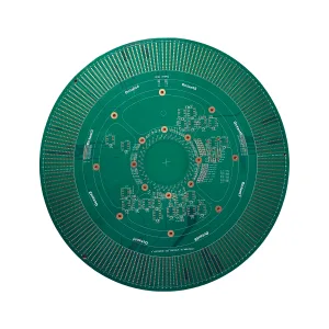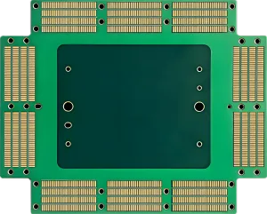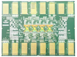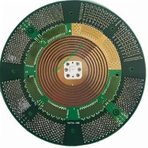
ATE Test Chip PCB Overview
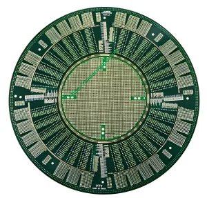
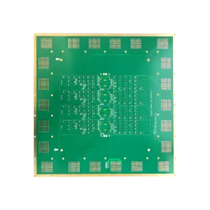
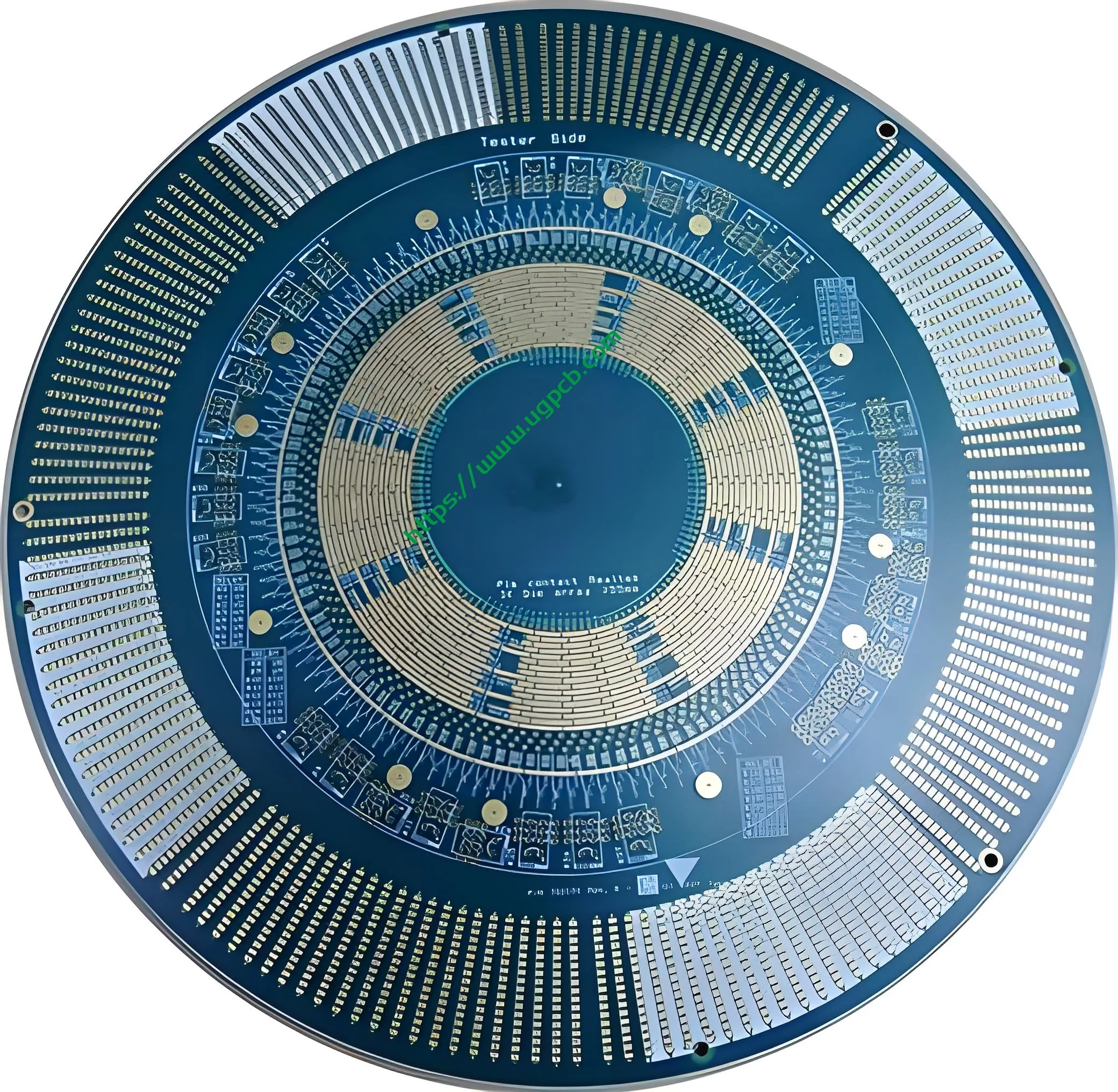
The ATE test chip PCB is a specialized placa de circuito impresso projetado para uso em equipamentos de teste automatizados (COMEU) systems for testing semiconductor chips. Esse PCB plays a crucial role in ensuring the quality and reliability of chips before they are integrated into electronic devices. Below is a detailed introduction to the ATE test chip PCB, cobrindo suas informações gerais, classificação, Materiais, desempenho, estrutura, características, processo de produção, e cenários de aplicação.
Classificação
ATE test chip PCBs are classified based on their layer count, Composição do material, e requisitos específicos de aplicação. O modelo apresentado aqui, ATE test chip PCB, is a 12-layer PCB, indicating its complexity and ability to handle intricate testing scenarios.
Composição de materiais
The ATE test chip PCB is constructed using isola 370hr material, um alto desempenho, high-reliability substrate known for its excellent electrical and thermal properties. This material ensures the PCB’s ability to withstand the demanding test conditions and provide stable performance.
Características de desempenho
The ATE test chip PCB excels in several performance areas, incluindo alta capacidade de transporte de corrente, baixa perda de sinal, e excelente gerenciamento térmico. The use of 2OZ copper thickness for inner layers and 1OZ for outer layers enhances its electrical conductivity and thermal dissipation capabilities. Adicionalmente, the immersion gold (5Você) surface finish provides superior corrosion resistance and solderability, ensuring reliable connections during testing.
Projeto Estrutural
Estruturalmente, the ATE test chip PCB features a board thickness of 3.0mm, providing a robust foundation for the complex circuitry and componentes. The green color not only adds a visual distinction but also aids in inspection and troubleshooting processes.
Características distintas
The ATE test chip PCB stands out with its unique features, including its high layer count, advanced material composition, and immersion gold surface finish. Esses recursos, combined with its precise design and manufacturing processes, make it an ideal choice for ATE chip testing applications.
Processo de Produção
The production of ATE test chip PCBs involves a series of sophisticated steps:
- Preparação de Materiais: The isola 370hr substrate is prepared and cut to the required dimensions.
- Laminação de cobre: A folha de cobre é laminada no substrato, with specific attention to the inner layer 2OZ and outer layer 1OZ thickness requirements.
- Padronização de circuito: Os padrões de circuito desejados são gravados na folha de cobre usando técnicas de gravação de precisão.
- Empilhamento e laminação de camadas: Múltiplas camadas são empilhadas e laminadas juntas, garantindo alinhamento e colagem precisos.
- Perfuração e Chapeamento: Furos são perfurados para montagem e interconexão de componentes, and then plated to enhance conductivity.
- Aplicação de acabamento superficial: The immersion gold (5Você) coating is applied to provide corrosion resistance and solderability.
- Inspeção e Testes Finais: O PCB passa por inspeção e testes rigorosos para garantir a conformidade com as especificações e requisitos de desempenho.
Cenários de aplicação
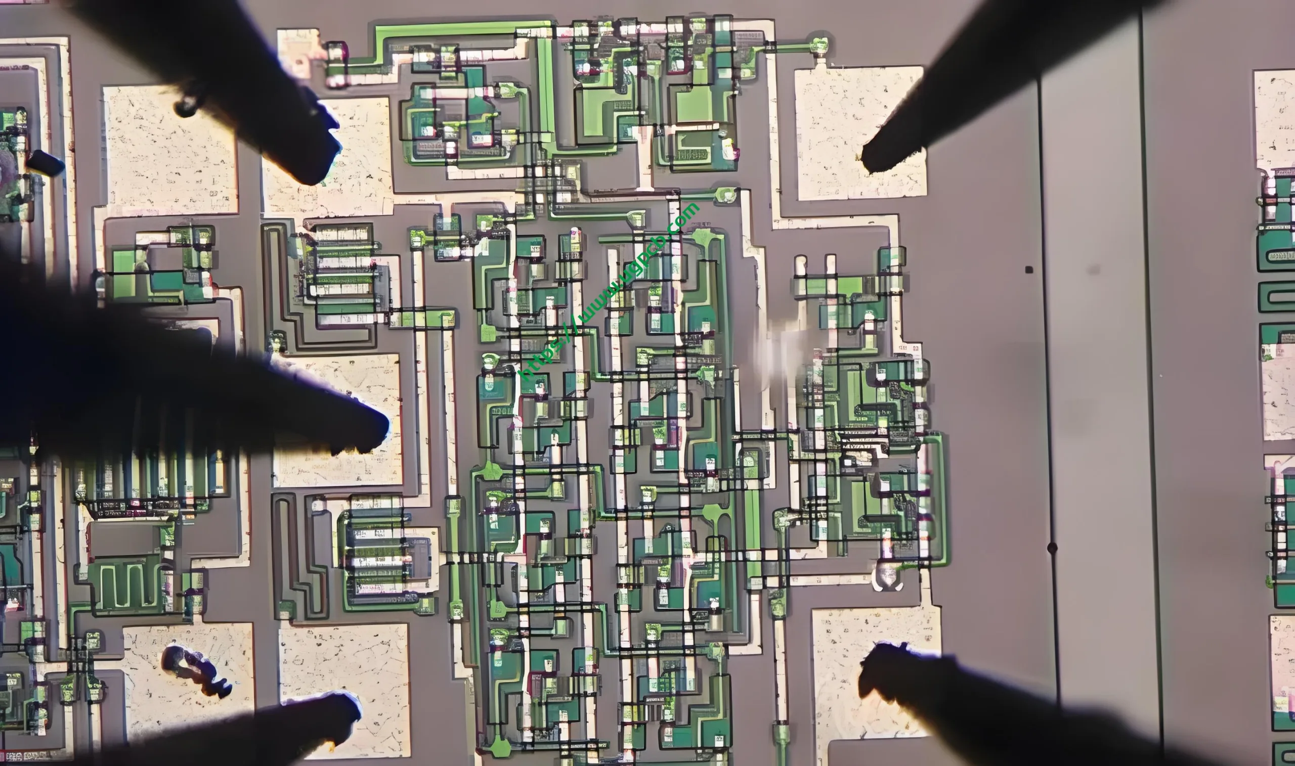
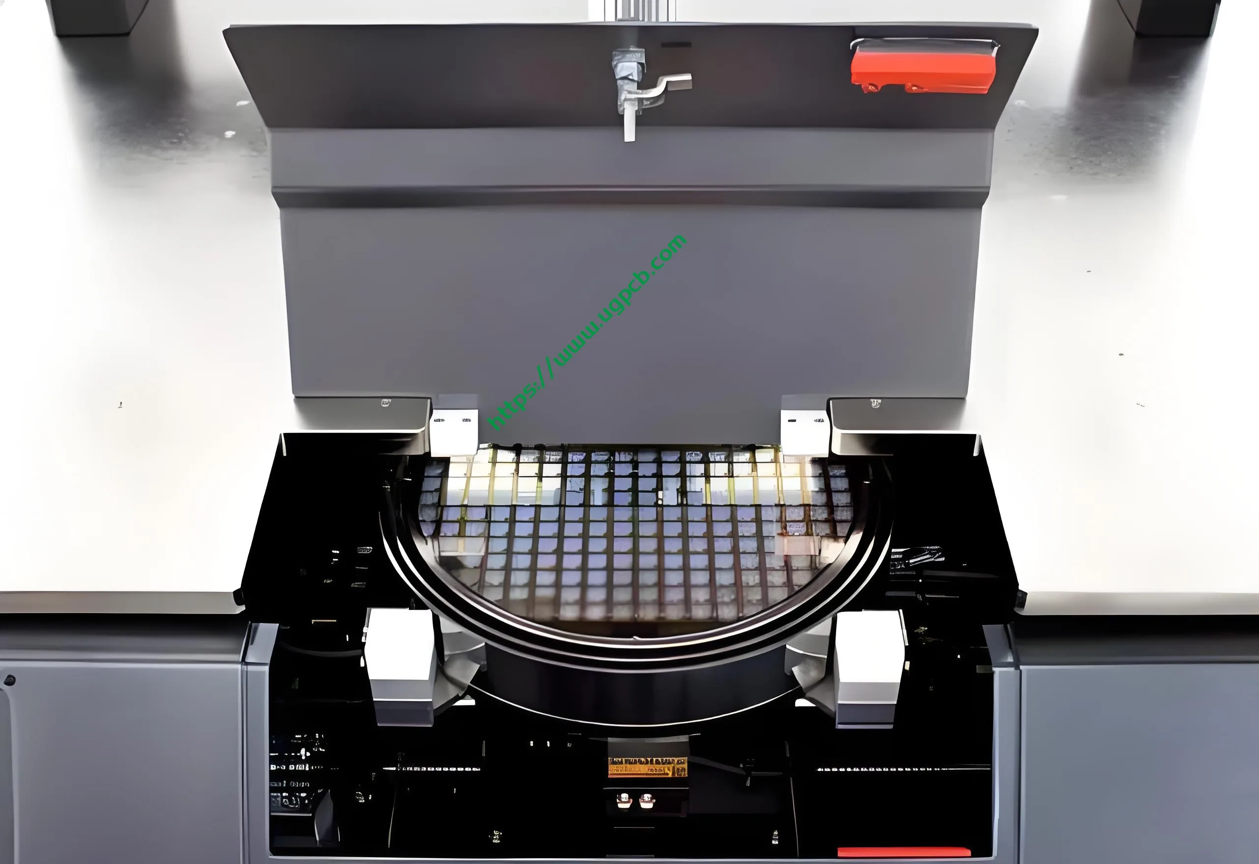
ATE test chip PCBs are primarily used in automated test equipment systems for the testing and validation of semiconductor chips. Eles são essenciais na indústria de semicondutores, where high-reliability testing is crucial for ensuring the quality and performance of chips before they are integrated into electronic devices. By utilizing ATE test chip PCBs, manufacturers can quickly and accurately identify any defects or issues in the chips, ensuring that only high-quality products are shipped to customers.