
UGPCB Bonding Circuit Board: A Premier Solution for High-Density IC Interconnection
In the world of compact and high-performance electronics, the demand for reliable interconnection solutions is paramount. UGPCB’s Bonding Circuit Board stands out as a specialized printed circuit board (PCB) designed specifically for intricate integrated circuit (CI) bonding processes. This product leverages high-precision manufacturing to meet the rigorous demands of modern semiconductor packaging and microelectronics.
Overview of the Bonding Circuit Board
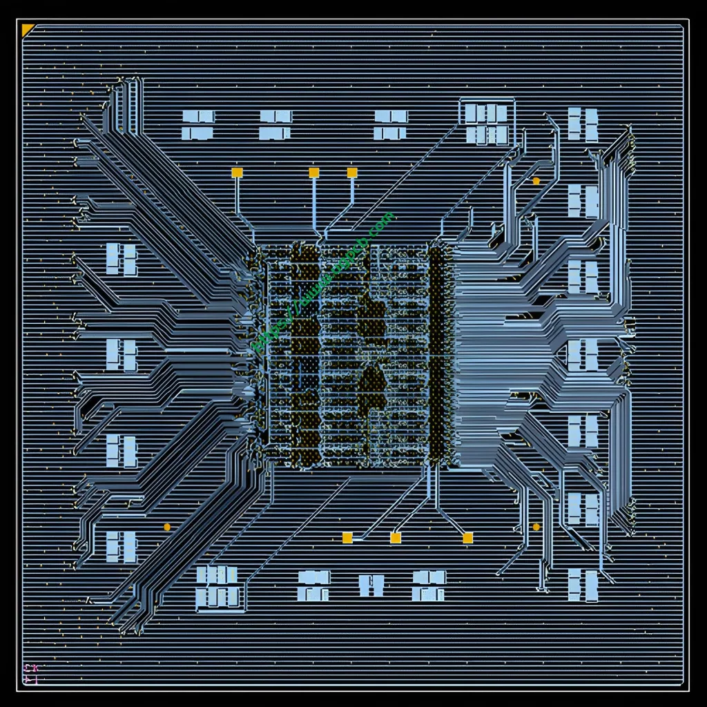
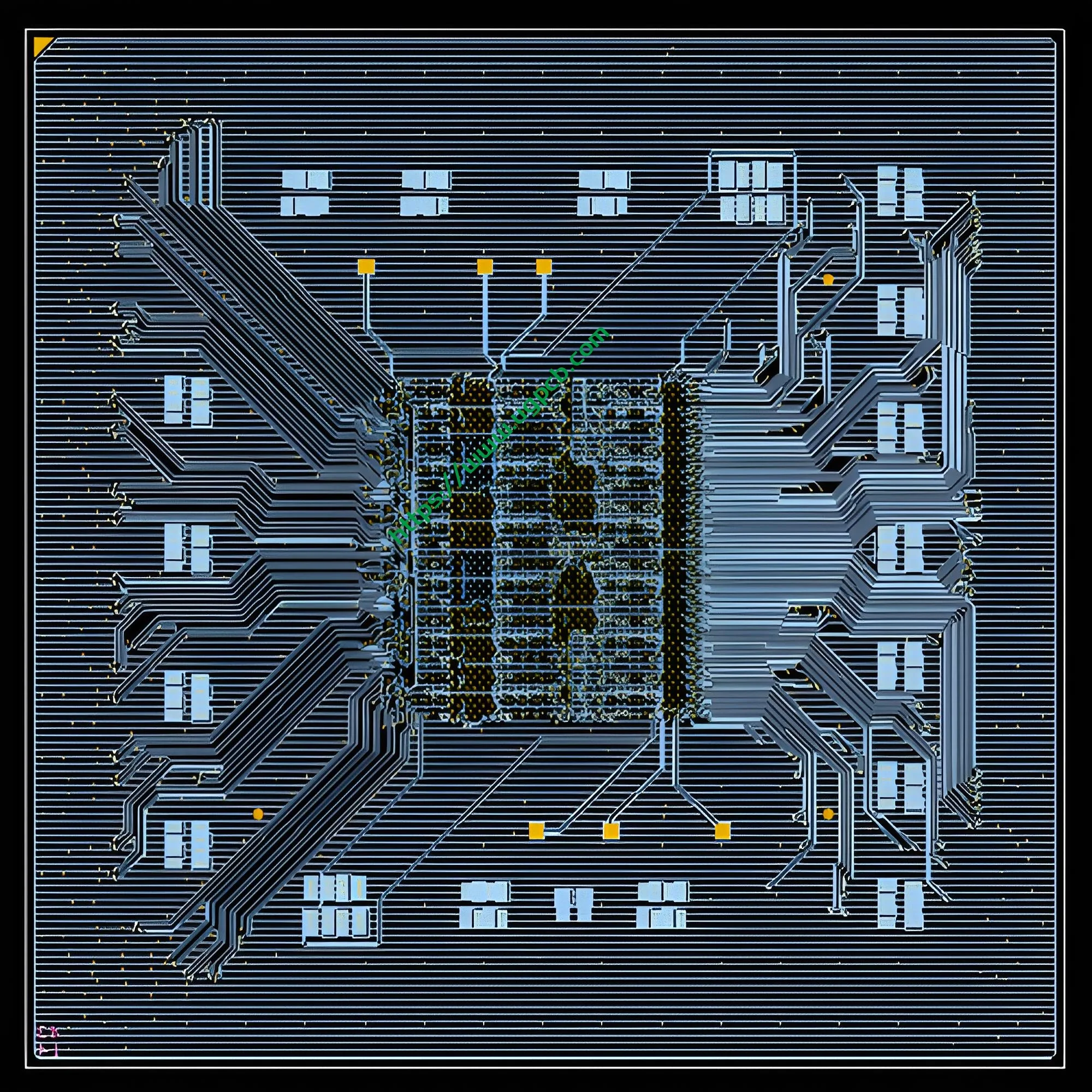
UGPCB’s Bonding Circuit Board is a high-density, double-layer PCB engineered to facilitate stable and precise wire bonding. Its core function is to serve as the substrate for mounting and electrically connecting semiconductor chips. With parameters like a 4mil trace/space and immersion gold surface finish, this PCB is tailored for applications where signal integrity and connection reliability are critical, making it an ideal choice for advanced PCB and PCBA (Conjunto da placa de circuito impresso) projects in the semiconductor sector.
What is a Bonding Circuit Board?
A Bonding Circuit Board is a specialized type of PCB that features ultra-fine circuitry and a meticulously prepared surface. Its primary role is to act as an interface platform where bare silicon chips are mounted and connected using fine wires through a process called wire bonding. This board is distinct from standard PCBs due to its superior surface planarity, minimal oxidation, and fine-line geometry, which are all essential for successful IC bonding and robust PCB assembly.
Key Design Considerations
The design of this bonding PCB is crucial for its performance. Several factors must be meticulously planned:
-
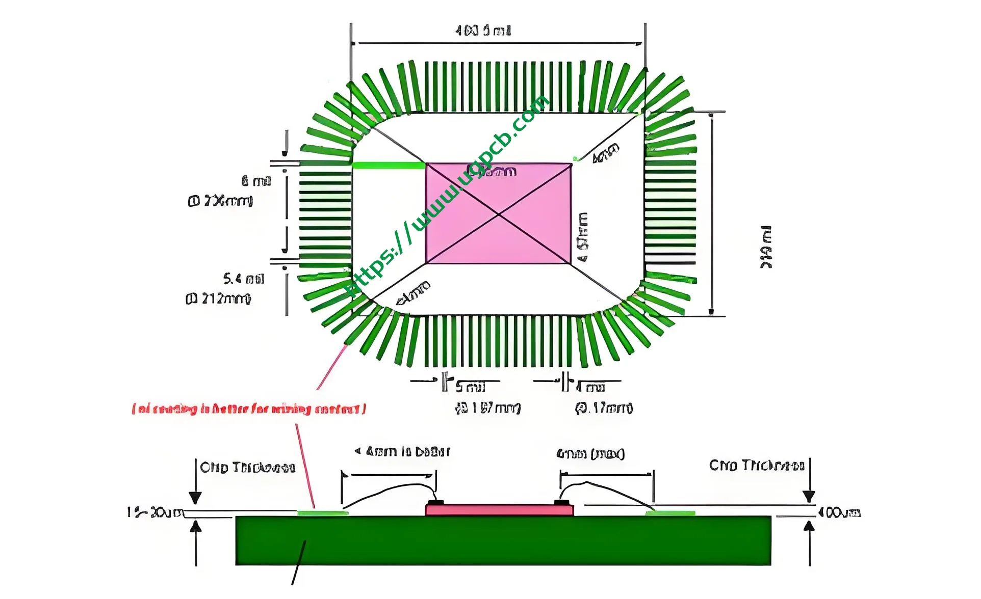
Traço e espaço: The minimum trace width and spacing of 4mil (approximately 0.1mm) allows for high-density interconnects, accommodating a large number of bonds in a small area.
-
Acabamento superficial: The Immersion Gold (CONCORDAR) treatment provides a flat, solderable, and oxidation-resistant surface that is perfect for the delicate wire bonding process.
-
Espessura do Cobre: At 0.5OZ, the copper offers a balance between carrying sufficient current and allowing for the creation of fine-line features.
-
Overall Thickness: A finished thickness of 1.0mm provides the necessary rigidity for handling during the PCBA and bonding processes while maintaining a compact profile.
How the Bonding Circuit Board Works
The principle of operation revolves around the wire bonding process. The semiconductor die is first attached to the bonding PCB. Então, using a specialized machine, extremely fine gold or aluminum wires are thermosonically or ultrasonically bonded between pads on the chip and corresponding pads on the PCB. The PCB’s circuitry then routes these signals to other components on the board, forming a complete electronic circuit. The immersion gold surface ensures a reliable, low-resistance connection point for every bond.
Primary Applications and Uses
This product is predominantly used in the semiconductor and microelectronics industries. Its main application is in IC Bonding for various devices, incluindo:
-
Sensor modules
-
Memory modules
-
RF and communication chips
-
Medical micro-devices
-
Unidades de controle automotivo
Classification of Bonding PCBs
Bonding PCBs can be classified based on several criteria. UGPCB’s model is specifically a:
-
Contagem de camadas: 2-camada PCB.
-
Material base: FR-4-based PCB.
-
Application-Specific: IC Bonding PCB or Chip-on-Board (Cobr) PCB.
Materials Used in Construction
The selection of materials directly impacts the board’s performance and reliability.
-
Base Laminate: FR-4 with a Glass Transition Temperature (Tg) of 130°C. This material offers excellent electrical insulation, força mecânica, and can withstand the thermal stress of the bonding and soldering processes.
-
Conductor: 0.5OZ (approximately 17.5µm) rolled or electro-deposited copper foil.
-
Acabamento superficial: Imersão Ouro, which consists of a thin layer of gold over a nickel barrier layer.
-
Máscara de solda: Green/White solder mask, which protects the copper traces and provides insulation.
Características de desempenho
The combination of materials and design results in a PCB with standout performance traits:
-
High Thermal Reliability: The Tg 130 FR-4 material ensures stability during high-temperature operations.
-
Excelente integridade do sinal: Fine traces and a consistent dielectric constant minimize signal loss and crosstalk.
-
Superior Bondability: The immersion gold finish offers a hard, flat surface that is ideal for consistent and strong wire bonds.
-
Durabilidade: The board is resistant to environmental factors like humidity and thermal cycling, ensuring long-term reliability in finished products.
Physical Structure of the Board
The board features a classic double-layer structure:
-
A core of FR-4 dielectric material.
-
A thin copper layer (0.5OZ) laminated on both the top and bottom sides.
-
A green or white solder mask applied over the copper, leaving only the bonding pads and solderable areas exposed.
-
A final immersion gold coating on the exposed pads, completing the 1.0mm thick board structure.
Distinguishing Features and Advantages
UGPCB’s Bonding Circuit Board offers several key benefits for PCB manufacturing and PCBA services:
-
High-Precision Circuitry: 4mil line/space capability supports complex, high-density designs.
-
Optimal Surface for Bonding: Immersion gold ensures a reliable connection interface for wire bonding.
-
Construção robusta: FR-4 Tg130 material provides excellent thermal and mechanical properties.
-
Cost-Effectiveness: A 2-layer design offers a perfect balance of performance and affordability for many bonding applications.
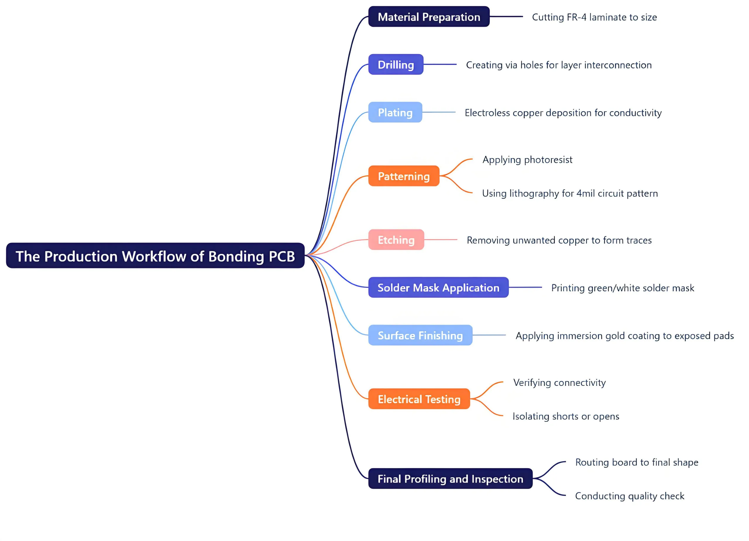
The Production Workflow
The manufacturing of this bonding PCB follows a rigorous process to ensure quality:
-
Preparação de Materiais: Cutting the FR-4 laminate to size.
-
Perfuração: Creating via holes for layer interconnection.
-
Revestimento: Electroless copper deposition to make hole walls conductive.
-
Patterning: Applying photoresist and using lithography to define the 4mil circuit pattern.
-
Gravura: Removing unwanted copper to form the precise traces.
-
Aplicação de máscara de solda: Printing the green/white solder mask.
-
Acabamento superficial: Applying the immersion gold coating to the exposed pads.
-
Teste elétrico: Verifying connectivity and isolating any shorts or opens.
-
Final Profiling and Inspection: Routing the board to its final shape and conducting a quality check.
Typical Usage Scenarios
This bonding PCB is typically deployed in environments that require high reliability and miniaturization. Common scenarios include:
-
Semiconductor Packaging Facilities: Where it is used in the assembly of BGA, QFN, and other advanced packages.
-
Montagem de PCB (PCBA) Lines: Integrated into larger systems as a sub-module hosting a critical IC.
-
Research and Development Labs: For prototyping new chip designs and interconnection technologies.
-
High-Volume Consumer Electronics Manufacturing: Used in devices like smartphones and wearables where space is at a premium.


