

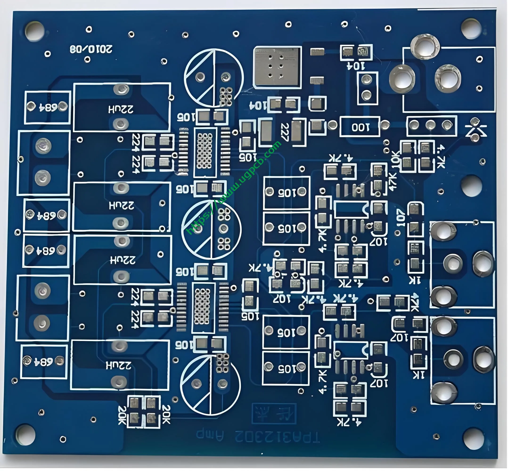
Introduction to UGPCB’s Double-Sided PCB for Relay Protection
UGPCB specializes in manufacturing high-performance double-sided Placas de circuito impresso (PCB) tailored for relay protection systems. These PCBs are engineered with FR-4 epoxy glass cloth as the base material, ensuring excellent electrical insulation and mechanical durability. Featuring a finished thickness of 1.6mm and a 1oz copper thickness (approximately 35μm), these boards support robust current-carrying capacity. O OSP (Conservador de solda orgânica) tratamento de superfície enhances solderability while protecting the copper pads from oxidation. With a minimum trace and spacing of 8mil (0.2milímetros), UGPCB’s designs achieve optimal signal integrity for precision-driven relay protection applications. Available in both black and white solder mask colors, these PCBs comply with CTI600 standards, offering high comparative tracking index performance to prevent electrical failures in humid conditions.
What Is a Double-Sided PCB?
UM PCB de dupla face incorporates conductive copper layers on both sides of an insulating substrate, como FR-4. The layers are interconnected using plated through-holes (PThs) ou vias, enabling complex circuitry in a compact form. Unlike single-sided PCBs, double-sided variants allow for higher component density and layout flexibility, making them ideal for intermediate-complexity devices like relay protection systems. These boards support double-sided assembly, including through-hole and surface-mount technologies (SMT), and are widely used in industrial, telecomunicações, e eletrônica automotiva.
Design Guidelines for Relay Protection PCBs
-
Trace Width and Spacing: UGPCB recommends a minimum of 8mil (0.2milímetros) for trace width and spacing to mitigate short-circuit risks and ensure signal clarity in high-voltage environments .
-
Thermal Relief Pads: Use cross-hatched thermal pads for large copper areas to dissipate heat during soldering, reducing the risk of virtual joints .
-
Via Specifications: For reliable interlayer connections, specify PTHs with a minimum finished hole diameter of 0.3mm and an annular ring of 0.7mm or larger .
-
Gridded Copper Planes: Implement gridded ground planes with a spacing ≥10mil to minimize PCB warping during wave soldering .
-
Solder Mask Details: Define solder mask openings precisely using the solder mask layer in design files to prevent bridging and expose thermal pads .
How Double-Sided PCBs Work in Relay Protection
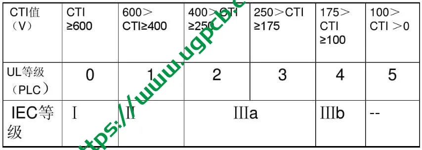
In relay protection systems, double-sided PCBs function as the central nervous system, monitoring electrical parameters and triggering disconnection during faults. The dual-layer layout facilitates the integration of current sensors, microprocessors, e módulos de comunicação. Por exemplo, traces on the top layer may carry low-voltage control signals, while the bottom layer handles high-current paths. Plated through-holes create low-impedance connections between layers, ensuring rapid fault detection and response. O CTI600-rated substrate resists conductive anode filament (CAF) formation, which is critical for longevity in high-humidity settings.
Applications of UGPCB’s Relay Protection PCBs
UGPCB’s double-sided PCBs are deployed in:
-
Power Grid Relay Systems: For overcurrent and earth fault protection.
-
Industrial Control Panels: Monitoring machinery in manufacturing plants.
-
Renewable Energy Inverters: Safeguarding solar/wind power converters.
-
Telecommunications Infrastructure: Protecting base station power supplies.
-
Railway Signaling Systems: Ensuring fail-safe track switching.
Classification of Double-Sided PCBs
-
Por material: FR-4 (padrão), CEM-3 (mid-range), and polyimide (high-temperature).
-
Por acabamento superficial: OSP (UGPCB’s default), Sangrar, CONCORDAR, and immersion tin.
-
By CTI Rating: CTI600 (like UGPCB’s boards), CTI400, and CTI600+ for harsh environments.
Materials and Construction
-
Material base: FR-4 glass epoxy is used for its flame-retardant properties (UL94V-0) and dielectric strength .
-
Folha de cobre: Electrolytic copper with 1oz thickness (35μm) per side .
-
Máscara de solda: Available in black or white, based on Taiyo PSR-4000 series, providing ≥10μm insulation thickness .
-
Acabamento superficial: OSP forms a protective organic layer on copper pads, ensuring solderability without lead .
Key Performance Metrics
-
Dielectric Strength: Withstands high voltages between conductive layers.
-
Thermal Endurance: Temperatura de transição vítrea (Tg) of 130–145°C prevents deformation under load .
-
CTI Rating: CTI600 guarantees resistance to tracking up to 600V.
-
Warpage Tolerance: Maximum warpage of 0.7% for SMT-assembled boards .
-
Plated Through-Hole Reliability: Copper plating ≥20μm in holes ensures uninterrupted interlayer connections .
Structure of a Double-Sided PCB
UGPCB’s PCBs feature:
-
Top and Bottom Copper Layers: 35μm thick, etched into circuit patterns.
-
FR-4 Core: A 1.6mm thick insulating substrate.
-
Plated Through-Holes: Metallized with copper for layer interconnection.
-
Solder Mask Layer: Applied over copper, excluding solderable pads.
-
Silkscreen Legend: White or black markings for component placement.
Advantages of UGPCB’s Design
-
Cost-Effectiveness: Reduces material expenses by 30–50% compared to multilayer alternatives.
-
Enhanced Design Flexibility: Supports cross-routing and optimized grounding schemes.
-
Improved Thermal Management: Gridded copper planes and thermal vias dissipate heat efficiently.
-
Alta confiabilidade: CTI600 and OSP finish extend service life in demanding conditions.
Manufacturing Process Overview
-
Preparação de Materiais: Cut FR-4 substrate to 510x610mm panels.
-
Perfuração: CNC drills create holes as small as 0.2mm for PTHs .
-
Electroless Copper Deposition: Catalytic oxidation builds a conductive layer in holes .
-
Pattern Imaging: Photolithography transfers circuit layouts using UV exposure.
-
Electroplating: Copper deposition thickens traces and hole walls to ≥20μm .
-
Gravura: Removes unwanted copper, defining traces.
-
Aplicação de máscara de solda: UV-curable ink printed and developed.
-
OSP Coating: Organic preservative applied to exposed copper.
-
Impressão de seda: Component indicators added.
-
Routing and V-Scoring: Panels separated into individual boards.

Common Usage Scenarios
-
Utility Substations: Housing protection relays for transformers and feeders.
-
Industrial Motor Drives: Embedding control logic for overload prevention.
-
Fontes de alimentação ininterruptas (UPS): Managing battery charge/discharge cycles.
-
Smart Meters: Enabling real-time energy monitoring.

Conclusão
UGPCB’s double-sided PCB boards for relay protection combine materiais avançados, precision engineering, and rigorous testing to deliver unmatched reliability. With features like FR-4 insulation, OSP coating, and CTI600 compliance, they are the optimal choice for critical power systems. Engineers seeking to enhance equipment safety and longevity can leverage UGPCB’s expertise for their next project.


