
High-Performance 12-Layer ENIG + Gold Finger PCB Visão geral do produto
O 12-Layer Gold Finger PCB is a hallmark product in the high-end placa de circuito impresso indústria, engineered specifically for electronic equipment demanding extreme reliability, stable electrical connections, and frequent plugging/unplugging cycles. UGPCB employs advanced manufacturing processes and premium materials (FR-4 TG170), combining 2μ” Ouro de imersão em níquel eletrolítico (CONCORDAR) surface finish with 30μ” Hard Gold Finger Plating tecnologia. We deliver a comprehensive high-reliability PCB solution for applications ranging from industrial controls to advanced communication systems.

Product Definition
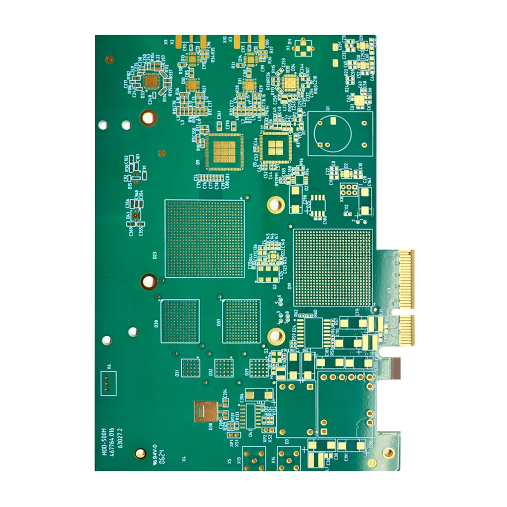
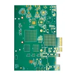
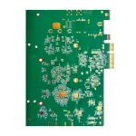
A Gold Finger PCB refers to a circuit board featuring a series of exposed, rectangular contact pads plated with thick gold (“fingers”) along one edge. These boards are designed for direct insertion into a matching connector slot, establishing a stable, pluggable connection for electrical signals and power between devices. This product is a 12-layer multilayer PCB with a standard thickness of 1.60milímetros, offering an optimal balance between complex circuit integration and mechanical robustness.
Critical Design Considerations
-
Gold Finger Area Design:
-
Chamfer (Bevel) Edge (Typically 20-45°): Facilitates smooth insertion into the connector—a critical aspect of Gold Finger Projeto de PCB.
-
Lead-in (Trace Fanout): Connections from the gold fingers to internal traces must have smooth curves, avoiding right angles to prevent stress concentration and plating cracks.
-
Solder Mask Clearance (Solder Mask Define): The gold finger area requires precise solder mask opening to ensure a clean, exposed plating surface.
-
-
Controle de impedância & Integridade do sinal: Como um 12-layer precision PCB, strict impedance control (por exemplo, 50Ω single-ended, 100Ω differential) for high-speed signal layers is essential. Stack-up design must be optimized via simulation to minimize crosstalk.
-
Thermal & Reliability Management: High-Tg material, coupled with a well-designed via structure, ensures the high-layer-count PCB operates stably in elevated temperature environments. Plated through-holes (PThs) should be avoided at the root of gold fingers to prevent fluid entrapment and structural weakness.
How It Works & Estrutura
This PCB facilitates complex circuit interconnections through its internal 12 conductive layers. The core functionality resides in the Hard Gold Plated Fingers. The durable 30-microinch gold plating provides excellent conductivity, oxidation resistance, e resistência ao desgaste. When the board is inserted into a backplane or card-edge connector, the gold fingers make tight, low-resistance electrical contact with the connector’s spring contacts, transmitting signals and power. The board core uses FR-4 TG170, providing solid mechanical support and electrical insulation.
Core Materials & Specifications
-
Material base: FR-4 TG170. A high-performance epoxy glass laminate.
-
High Glass Transition Temperature (Tg ≥ 170°C): Significantly enhances the PCB’s mechanical stability and heat resistance under high-temperature operating conditions, preventing delamination and Z-axis expansion.
-
Superior Electrical Properties: Constante dielétrica baixa (Dk) and dissipation factor (Df), suitable for mid-to-high frequency applications.
-
High Mechanical Strength: Ensures the 1.6mm thick PCB board resists bending and warping in mating/unmating and high-vibration environments.
-
-
Acabamentos de superfície:
-
Board Surface: Ouro de imersão em níquel eletrolítico (CONCORDAR, 2μ”): Provides a flat, coplanar surface for reliable soldering of fine-pitch components and offers excellent oxidation resistance.
-
Gold Fingers: Selective Electroplated Hard Gold (30μ”): High hardness, superior abrasion resistance, and extended mating cycle life, capable of withstanding 500+ insertion/withdrawal cycles with ease.
-
Key Features & Vantagens
-
Unmatched Reliability: FR-4 TG170 high-Tg material e 12-layer precision lamination ensure long-term stability in harsh operating conditions.
-
Extended Mating Cycle Life: 30μ” thick hard gold fingers far exceed standard plating thickness, offering exceptional wear resistance—the ideal choice for high-durability plug-in PCBs.
-
Excelente integridade do sinal: The multilayer design provides uninterrupted reference planes for high-speed signals, and controlled impedance guarantees signal quality.
-
Robust Thermal & Mechanical Performance: The 1.60mm standard thickness combined with high-Tg material delivers superior rigidity, Gerenciamento térmico, and dimensional stability.
-
Comprehensive High-End Solution: De multicamada Fabricação de PCB para specialty surface finishing (CONCORDAR + Selective Gold), UGPCB provides full-process control, ensuring consistent, high-quality results.
Manufacturing Process Flow
Panelization → Inner Layer Imaging → Lamination (12-Camada) → Drilling → Desmear & Electroless Copper Deposition → Outer Layer Imaging → Pattern Plating (for Hard Gold Fingers) → Etching → Solder Mask Application → ENIG Surface Finish → Gold Finger Beveling → Electrical Test (Sonda Voadora / Fixture) → Final Automated Optical Inspection (AOI) → Packaging.
Aplicações primárias & Casos de uso
This product is the core component of high-end electronic devices requiring direct board-to-board plug connections ou integration into backplane systems.
-
Industrial Control Systems: PLC modules, industrial computer motherboards, servo drives, I/O interface cards.
-
Telecomunicações & Networking Equipment: Router/switch line cards, optical transceiver modules, baseband processing units.
-
Eletrônica médica: Data acquisition and processing boards for advanced medical imaging systems (por exemplo, Tomógrafos, ultrasound machines).
-
Test & Measurement Instruments: Plug-in modules for high-end oscilloscopes, spectrum analyzers, and Automated Test Equipment (COMEU).
-
Aeroespacial & Defense Electronics: Mission-critical avionics systems and radar signal processing modules where reliability is paramount.

Scientific Product Classification
-
Por contagem de camadas: High-Layer-Count / Multilayer Circuit Board (≥8 layers, especificamente 12 camadas).
-
By Special Feature/Process: Gold Finger (Gold Edge Connector) PCB, Mixed Surface Finish PCB (CONCORDAR + Selective Hard Gold).
-
By Material Property: Alta Tg (TG170) PCB, FR-4 Series PCB.
-
By Application Grade: Industrial-Grade PCB, Telecom-Grade PCB, High-Reliability PCB.
Why Choose UGPCB’s 12-Layer Gold Finger PCB?
We understand that a reliable Gold Finger PCB is the foundation of your high-end equipment’s stable operation. Leveraging deep expertise in multicamada Fabricação de placas de circuito impresso e specialty surface finish processes, UGPCB guarantees that every board delivered meets military-grade reliability standards with commercial-grade delivery efficiency. We provide not just a product, but a customized PCB solution.
Contact our technical sales team today to discuss your project requirements, receive a detailed quote, and qualify for a free design-for-manufacturability (Dfm) review and sample program. Partner with UGPCB for your most demanding 12 layer circuit board Aplicações.


