

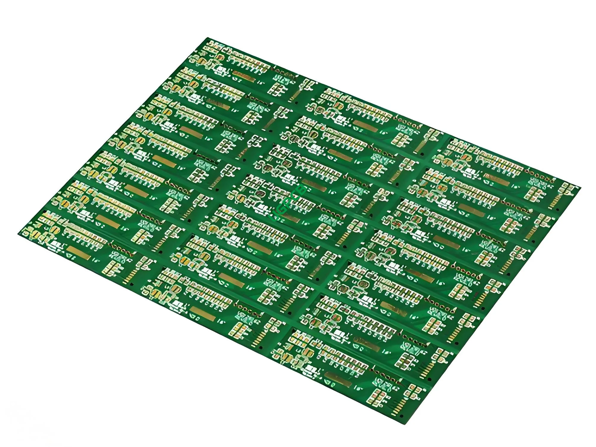
Overview of the P2.9 LED Printed Circuit Board
The P2.9 LED Printed Circuit Board (PCB) is a specialized PCB designed for use with P2.9 LED modules, which are commonly used in high-resolution display applications. This PCB is ideal for creating large, seamless LED displays.
What is a P2.9 LED Printed Circuit Board?
A P2.9 LED Printed Circuit Board is a placa de circuito impresso (PCB) specifically designed to accommodate and connect P2.9 LED modules. O termo “P2.9” refers to the pixel pitch of the LED module, which measures 2.9 millimeters between each pixel. This PCB ensures that the LED modules can be interconnected efficiently, providing a stable platform for the electronic components.
Requisitos de design
The design requirements for a P2.9 LED Printed Circuit Board are stringent to ensure its performance and reliability:
- Material: SY1000-2 TG170 FR4, chosen for its excellent electrical and thermal properties.
- Contagem de camadas: 6 layers to accommodate the necessary circuitry and signal integrity.
- Cor: Preto/branco para fácil identificação e apelo estético.
- Espessura Acabada: 1.0mm to provide structural integrity and durability.
- Espessura do Cobre: 1OZ to ensure adequate conductivity and heat dissipation.
- Tratamento de superfície: O ouro de imersão para melhorar a solda e a resistência à corrosão.
- Traço mínimo e espaço: 4mil(0.1milímetros) Para suportar padrões de circuito fino.
- Característica: More pads with small spacing to accommodate the dense layout of P2.9 LED modules.
Como funciona?
The P2.9 LED Printed Circuit Board works by providing a platform for various electronic components to be interconnected through conductive pathways. Esses caminhos, ou traços, são feitos de cobre e são gravados no quadro. The SY1000-2 TG170 FR4 material ensures that the PCB can withstand the demands of LED display applications, while the immersion gold surface treatment ensures that these traces remain conductive and resistant to corrosion.
Aplicações
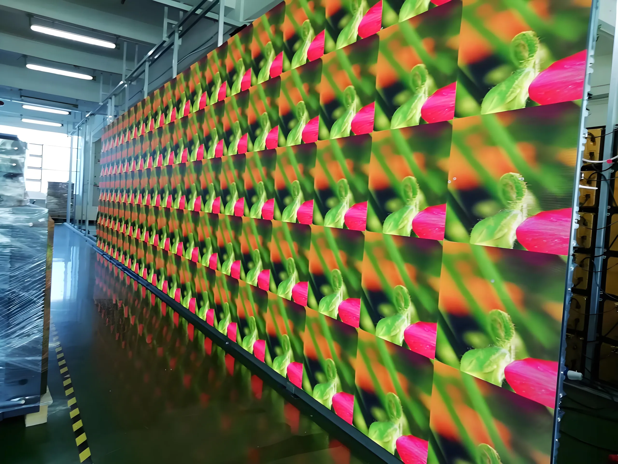
The primary application of the P2.9 LED Printed Circuit Board is in high-resolution LED display systems where it manages and regulates the flow of electrical signals. Isso inclui:
- Indoor and outdoor LED displays
- Digital signage
- Large format video walls
- Event stages and concert screens
Classificação
Com base em seus recursos e aplicativos, the P2.9 LED Printed Circuit Board can be classified as a high-density, high-speed digital PCB designed for LED display applications. This classification highlights its capability to handle high-frequency signals and provide stable electrical connections.
Composição de materiais
The core material used in the P2.9 LED Printed Circuit Board is SY1000-2 TG170 FR4, a high-performance composite material known for its excellent mechanical, térmico, e propriedades elétricas. This material ensures that the PCB can withstand the demands of LED display applications.
Características de desempenho
The performance characteristics of the P2.9 LED Printed Circuit Board include:
- Alta integridade do sinal
- Baixa perda de sinal
- Gerenciamento térmico superior
- Força mecânica robusta
- Estabilidade a longo prazo
Detalhes estruturais
The structural details of the P2.9 LED Printed Circuit Board are as follows:
- Contagem de camadas: 6 camadas
- Espessura Acabada: 1.0milímetros
- Espessura do Cobre: 1OZ
- Tratamento de superfície: Imersão Ouro
- Traço mínimo e espaço: 4mil(0.1milímetros)
- Característica: More pads with small spacing to accommodate the dense layout of P2.9 LED modules.
Recursos e benefícios
The key features and benefits of the P2.9 LED Printed Circuit Board include:
- Interconectividade de alta densidade
- Excelente integridade do sinal
- Construção mecânica robusta
- Desempenho confiável de longo prazo
- Opções de cores estéticas (Preto/branco)
Processo de Produção
The production process of the P2.9 LED Printed Circuit Board involves several steps including:
- Seleção de material: Choosing high-quality SY1000-2 TG170 FR4 material.
- Empilhamento de camada: Organizando o 6 camadas com precisão.
- Gravura: Removendo o excesso de cobre para formar os padrões de traços desejados.
- Aplicação de máscara de solda: Applying a solder mask layer to protect the copper traces.
- Revestimento: Aplicando tratamento de superfície de ouro de imersão.
- Conjunto: Incorporando PTHs e Vias para interconexões de camada.
- Teste: Garantir que o PCB atenda a todas as especificações de desempenho.
Casos de uso
The P2.9 LED Printed Circuit Board is used in various scenarios such as:
- High-resolution indoor and outdoor LED displays
- Digital signage installations
- Concert and event stages with large video walls
- Retail environments with dynamic advertising screens


