

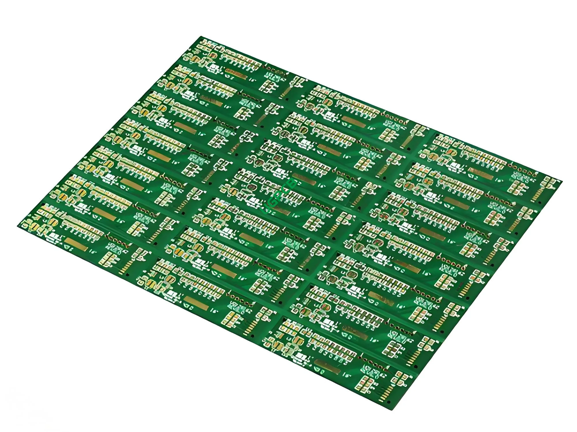
Overview of the P2.9 LED Printed Circuit Board
The P2.9 LED Printed Circuit Board (PCB) is a specialized PCB designed for use with P2.9 LED modules, which are commonly used in high-resolution display applications. This PCB is ideal for creating large, seamless LED displays.
What is a P2.9 LED Printed Circuit Board?
A P2.9 LED Printed Circuit Board is a placa de circuito impresso (PCB) specifically designed to accommodate and connect P2.9 LED modules. O termo “P2.9” refers to the pixel pitch of the LED module, which measures 2.9 millimeters between each pixel. This PCB ensures that the LED modules can be interconnected efficiently, providing a stable platform for the electronic components.
Requisitos de design
The design requirements for a P2.9 LED Printed Circuit Board are stringent to ensure its performance and reliability:
- Material: SY1000-2 TG170 FR4, escolhido por suas excelentes propriedades elétricas e térmicas.
- Contagem de camadas: 6 layers to accommodate the necessary circuitry and signal integrity.
- Cor: Preto/branco para fácil identificação e apelo estético.
- Espessura Acabada: 1.0mm para fornecer integridade estrutural e durabilidade.
- Espessura do Cobre: 1OZ para garantir condutividade adequada e dissipação de calor.
- Tratamento de superfície: O ouro de imersão para melhorar a solda e a resistência à corrosão.
- Traço mínimo e espaço: 4mil(0.1milímetros) Para suportar padrões de circuito fino.
- Característica: More pads with small spacing to accommodate the dense layout of P2.9 LED modules.
Como funciona?
The P2.9 LED Printed Circuit Board works by providing a platform for various electronic components to be interconnected through conductive pathways. Esses caminhos, ou traços, são feitos de cobre e são gravados no quadro. The SY1000-2 TG170 FR4 material ensures that the PCB can withstand the demands of LED display applications, enquanto o tratamento de superfície de ouro por imersão garante que esses vestígios permaneçam condutores e resistentes à corrosão.
Aplicações
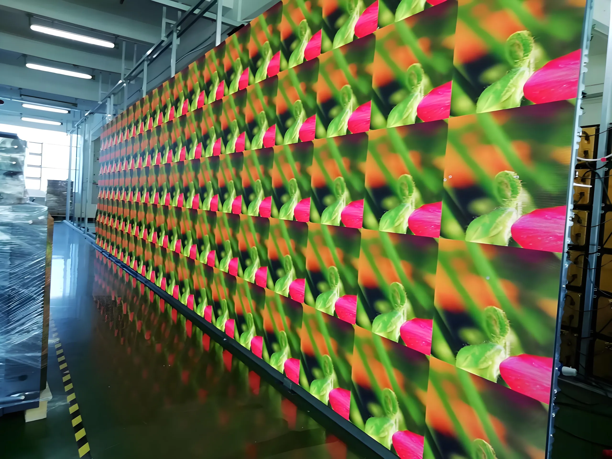
The primary application of the P2.9 LED Printed Circuit Board is in high-resolution LED display systems where it manages and regulates the flow of electrical signals. Isso inclui:
- Indoor and outdoor LED displays
- Digital signage
- Large format video walls
- Event stages and concert screens
Classificação
Com base em seus recursos e aplicativos, the P2.9 LED Printed Circuit Board can be classified as a high-density, high-speed digital PCB designed for LED display applications. Esta classificação destaca sua capacidade de lidar com sinais de alta frequência e fornecer conexões elétricas estáveis.
Composição de materiais
O núcleo material used in the P2.9 LED Printed Circuit Board is SY1000-2 TG170 FR4, um material compósito de alto desempenho conhecido por seu excelente desempenho mecânico, térmico, e propriedades elétricas. This material ensures that the PCB can withstand the demands of LED display applications.
Características de desempenho
The performance characteristics of the P2.9 LED Printed Circuit Board include:
- Alta integridade do sinal
- Baixa perda de sinal
- Gerenciamento térmico superior
- Força mecânica robusta
- Estabilidade a longo prazo
Detalhes estruturais
The structural details of the P2.9 LED Printed Circuit Board are as follows:
- Contagem de camadas: 6 camadas
- Espessura Acabada: 1.0milímetros
- Espessura do Cobre: 1OZ
- Tratamento de superfície: Imersão Ouro
- Traço mínimo e espaço: 4mil(0.1milímetros)
- Característica: More pads with small spacing to accommodate the dense layout of P2.9 LED modules.
Recursos e benefícios
The key features and benefits of the P2.9 LED Printed Circuit Board include:
- Interconectividade de alta densidade
- Excelente integridade do sinal
- Construção mecânica robusta
- Desempenho confiável de longo prazo
- Opções de cores estéticas (Preto/branco)
Processo de Produção
The production process of the P2.9 LED Printed Circuit Board involves several steps including:
- Seleção de material: Choosing high-quality SY1000-2 TG170 FR4 material.
- Empilhamento de camada: Organizando o 6 camadas com precisão.
- Gravura: Removendo o excesso de cobre para formar os padrões de traços desejados.
- Aplicação de máscara de solda: Applying a solder mask layer to protect the copper traces.
- Revestimento: Aplicando tratamento de superfície de ouro de imersão.
- Conjunto: Incorporando PTHs e Vias para interconexões de camada.
- Teste: Garantir que o PCB atenda a todas as especificações de desempenho.
Casos de uso
The P2.9 LED Printed Circuit Board is used in various scenarios such as:
- High-resolution indoor and outdoor LED displays
- Digital signage installations
- Concert and event stages with large video walls
- Retail environments with dynamic advertising screens


