Overview of MAX2829 Transceiver
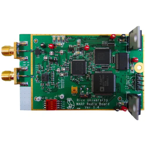
The WARP radio board utilizes a dual-band direct conversion radio transceiver from Maxim, o MAX2829. This transceiver supports both the 2.4 Ghz e 5 GHz ISM bands. Although it is intended for use in 802.11a/b/g/n designs, this transceiver provides a flexible analog baseband interface. This interface allows the translation of any waveform, with a bandwidth up to 40 MHz, between baseband and RF, regardless of the waveform’s adherence to an 802.11 padrão.
Phase Coherency in MIMO Applications
Further, when driven by a common reference clock, the phase coherency of the local oscillators in multiple MAX2829 transceivers is guaranteed. This feature is critical in MIMO applications as many algorithms require carefully controlled phase relationships and accurate measurements of phase among multiple antennas.
WARP Radio Board Components
RF Chain
WARP radio board
- The WARP radio board’s RF chain is completed by bandpass filters, a dual-band power amplifier, and a Tx/Rx switch.
- The amplifier in the current design is capable of transmitting OFDM waveforms at 18 dbm. Future revisions of the board will likely incorporate more powerful amplifiers which will be better suited to long-range, outdoor deployment.
Projeto de PCB
- The WARP radio board is a 6-layer, 2×3″ (4.5x7cm) PCB.
- The board houses all of the components necessary to provide a purely digital interface to the host board’s FPGA.
- Dedicated linear power regulators are also used to meet the low noise requirements of the data converters and RF transceiver.
- The RF signals are routed to board-edge connectors to provide flexibility in the selection and arrangement of antennas.
Hardware and Software Cores
Adicionalmente, we provide hardware and software cores to enable the use of this daughtercard. The cores implement the details to control all devices on the board, allowing the user to call C functions to perform the various processes in a communications system.
By incorporating the MAX2829 transceiver and designing a versatile PCB, the WARP radio board is well-suited for a wide range of communications applications.