
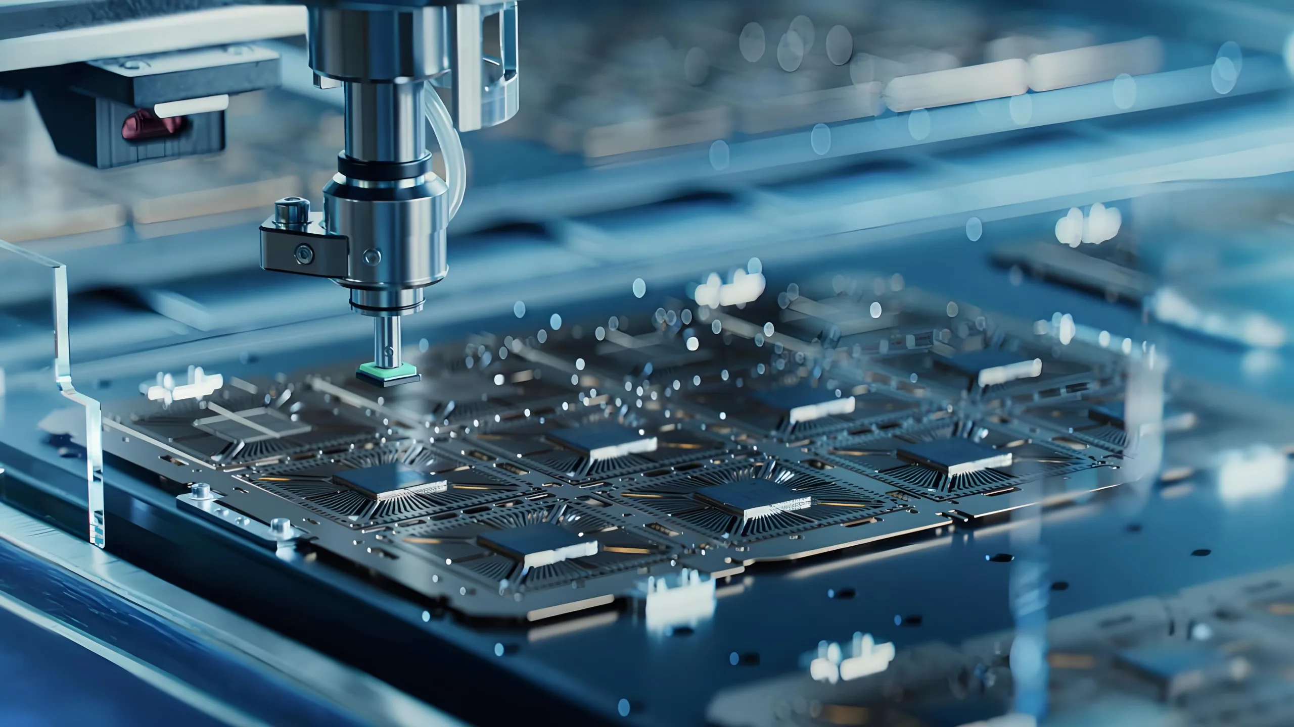
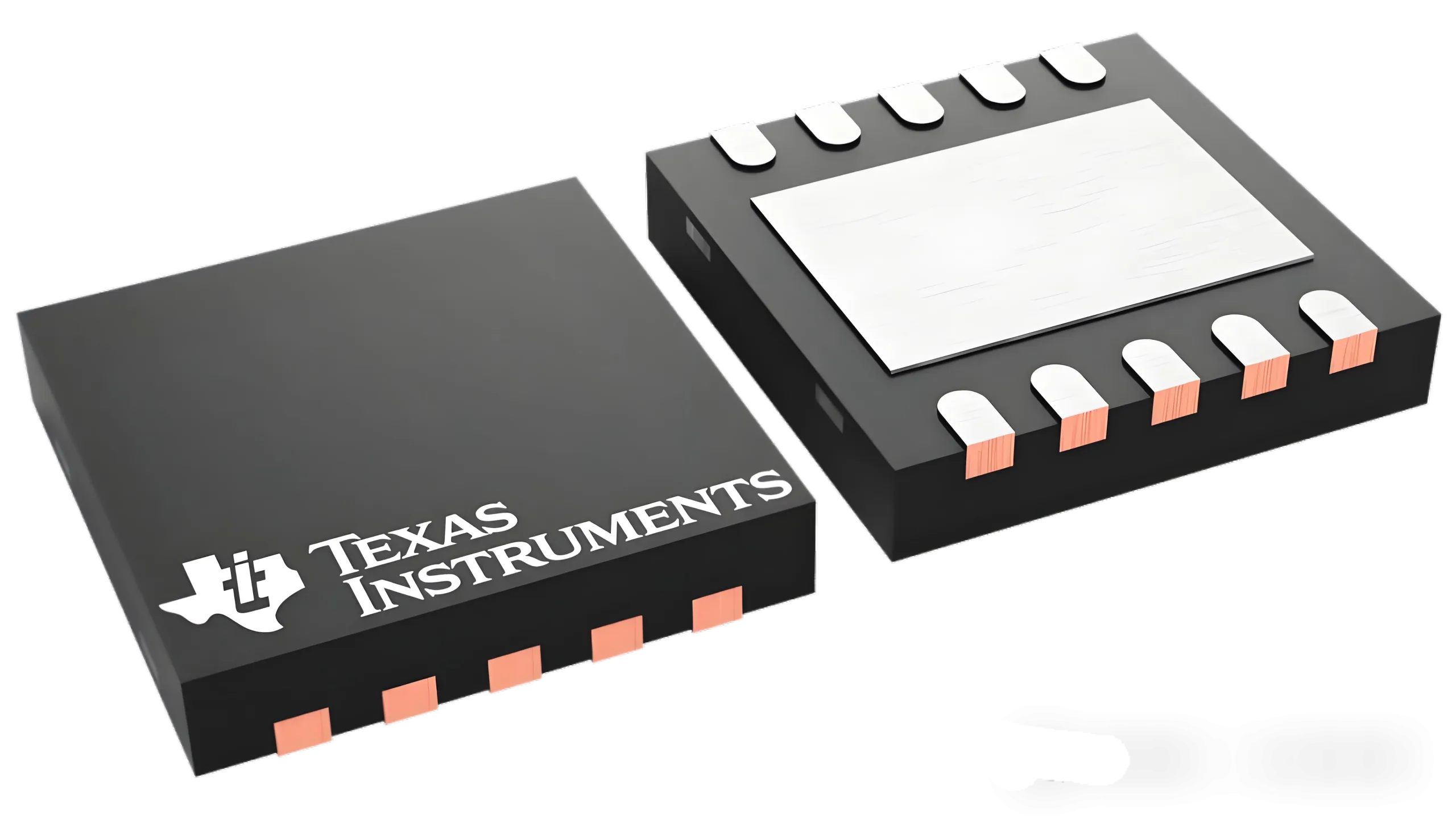
ชิปเซมิคอนดักเตอร์ทำหน้าที่เป็น “สมอง” ของยุคดิจิตอล, ในขณะที่ชิปบรรจุภัณฑ์ทำหน้าที่ป้องกันของพวกเขา “เกราะ” และ “เครือข่ายประสาท” นอกเหนือจากการป้องกันซิลิคอนที่เปราะบาง, ช่วยให้การจัดการความร้อนที่สำคัญ, การเชื่อมต่อไฟฟ้า, และการส่งสัญญาณ. ตั้งแต่แพ็คเกจผ่านรูขนาดใหญ่ไปจนถึงโซลูชันระดับเวเฟอร์บางเฉียบ, Evolution Packaging ได้ขับเคลื่อนการย่อขนาดเล็กและการเพิ่มประสิทธิภาพของอิเล็กทรอนิกส์ - Saga เทคโนโลยีอนุสาวรีย์.
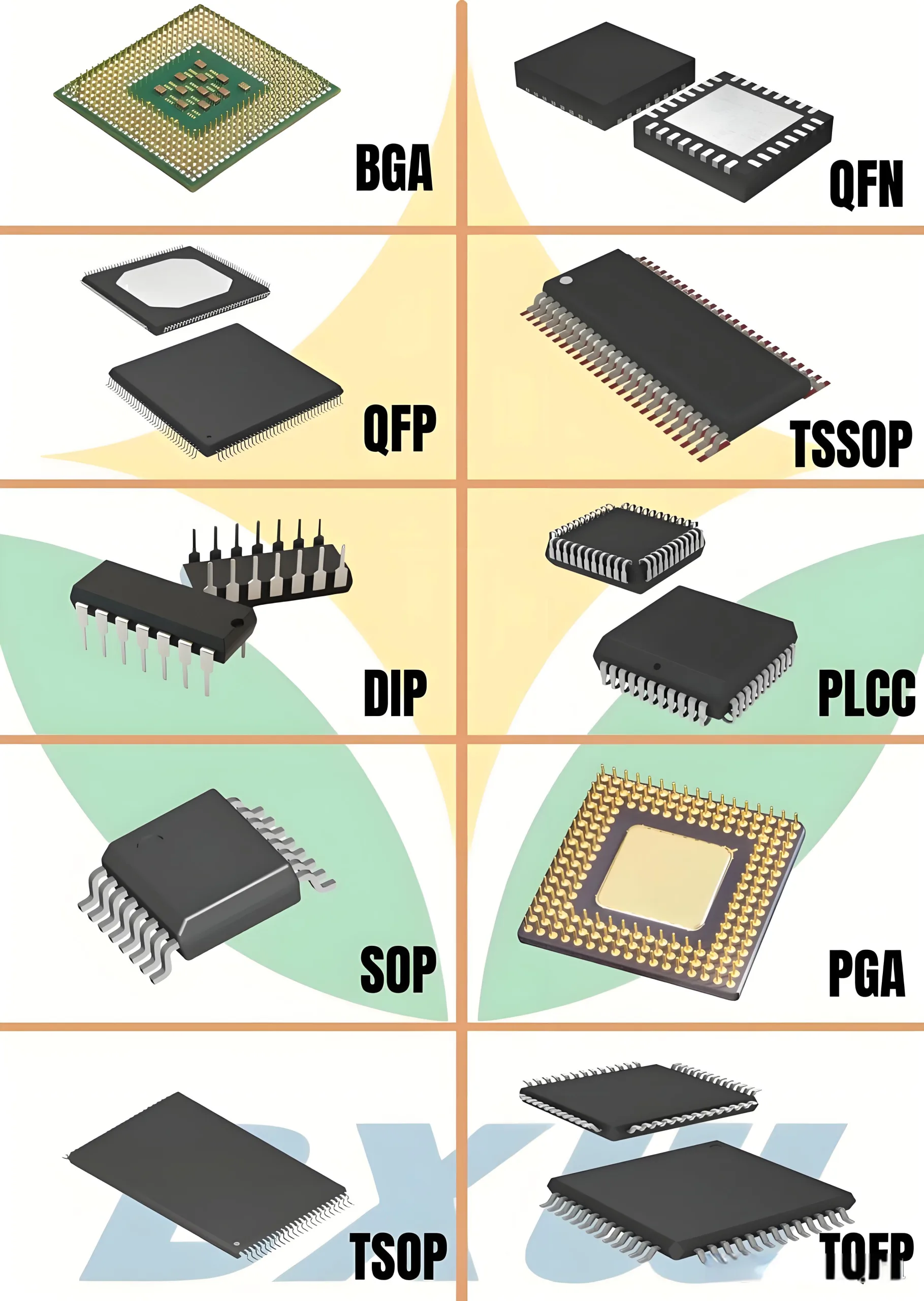
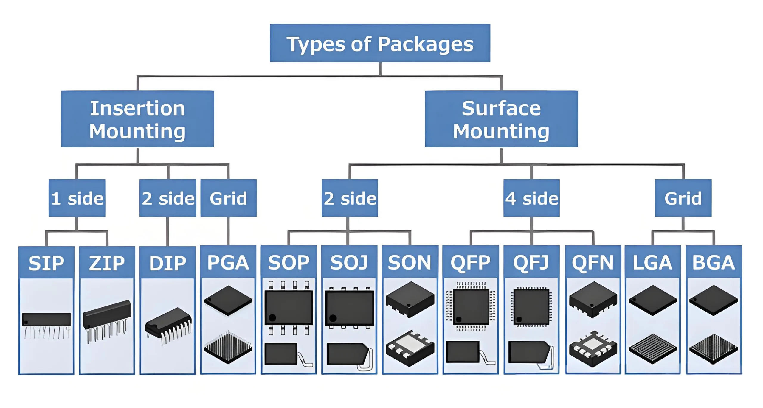
การจำแนกเทคโนโลยีบรรจุภัณฑ์
โดยวิธีการติดตั้ง
-
บรรจุภัณฑ์ผ่านหลุม (tht):
หมุดใส่เข้าไปใน พีซีบี ชุบผ่านหลุมสำหรับการบัดกรี. แสดงถึงเทคโนโลยียุคต้น ๆ. -
เทคโนโลยีพื้นผิว (SMT):
ส่วนประกอบบัดกรีลงบนแผ่น PCB โดยตรง. ช่วยให้ความหนาแน่นสูงขึ้นและการประกอบอัตโนมัติ.
โดยการกำหนดค่า PIN (ความหนาแน่น)
แถวเดียว→ Dual-row → Quad-Sided → Area-Array
ยุคผ่านรู
ทำ/ถึง: รากฐานของส่วนประกอบที่ไม่ต่อเนื่อง
-
DO-41 ไดโอด: Ø2.7มม. × 5.2 มม.
-
TO-220 ทรานซิสเตอร์: จัดการการกระจายพลังงาน≤50W
-
ความต้านทานความร้อน: R<ส่วนย่อย>และ</ส่วนย่อย> - (T<ส่วนย่อย>J</ส่วนย่อย> – T<ส่วนย่อย>อัน</ส่วนย่อย>)/P
ที่ไหน R<ส่วนย่อย>และ</ส่วนย่อย> = ความต้านทานความร้อนทางแยกไปยังแอมป์
จิบ/ซิป: นวัตกรรมเดียวในบรรทัด
-
จิบ: 3-16 หมุด, คุ้มค่าสำหรับตัวต้านทาน/ไดโอดพลังงานต่ำ
-
ซิป: 40% ความหนาแน่นของพินสูงกว่า SIP ผ่านการจัดเรียงพินซิกแซก
-
การใช้งาน: โมดูลหน่วยความจำก่อน, หน่วยงานกำกับดูแลแรงดันไฟฟ้า
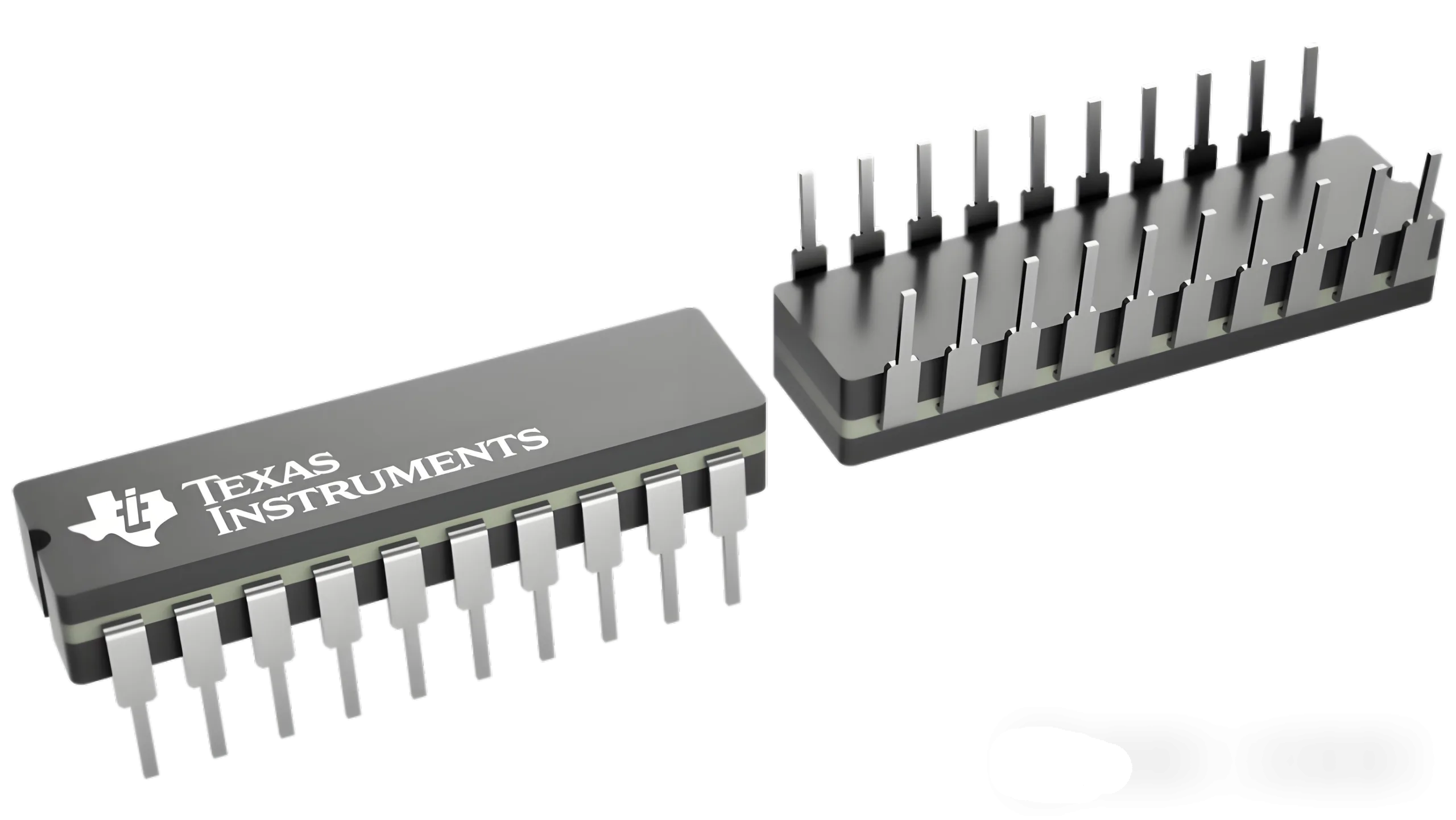
จุ่ม: การปฏิวัติ IC
-
พิทช์: 2.54มม (0.1″) มาตรฐาน
-
1980ส่วนแบ่งการตลาด: >70% ของบรรจุภัณฑ์ IC
-
ประสิทธิภาพความร้อน:
จุ่มเซรามิก: 20-30 w/m ·ค่าการนำไฟฟ้า k
พลาสติกจุ่ม: 0.2-0.3 w/m · k
PGA: ผู้บุกเบิกการคำนวณประสิทธิภาพสูง
-
ความหนาแน่นของพิน: 3×สูงกว่าการจุ่ม
-
การใช้งาน: Intel 80386/80486 ซีพียู
-
กำลังแทรก: 30-100 นิวตัน
การปฏิวัติ SMT
SOD/SOT: การย่อส่วนประกอบที่ไม่ต่อเนื่อง
-
SOD-323: 1.7mm × 1.25 มม.
-
ความต้านทานความร้อน SOT-23: ~ 250 ° C/W
-
โปรไฟล์การรีมอน: อุณหภูมิสูงสุด 235-245 ° C
ผู้นำปีกนางนวล: ครอบครัว SOP
-
วิวัฒนาการพิทช์พิท:
1.27มม (จู่โจม) → 0.8 มม. (SSOP) → 0.65 มม. (TSSOP) -
แพ็คเกจอนุพันธ์:
SOP → SSOP → TSOP → TSSOP → VSSOP -
การเพิ่มความร้อน: HSSOP ลดความต้านทานความร้อนโดย 40%
การกำหนดค่า J-Lead: การสังเกตการณ์
-
ความแข็งแรงเชิงกล: 30% ความต้านทานต่อความเครียดที่สูงขึ้น
-
ข้อ จำกัด ไฟฟ้า: 0.8-1.2การเหนี่ยวนำของ NH Parasitic
ความก้าวหน้าแบบไม่เป็นไปได้: ลูกชาย/dfn
-
ประสิทธิภาพพื้นที่: >50% ปรับปรุง SOP
-
ประสิทธิภาพความร้อน: 15° C/W พร้อมแผ่นความร้อน
-
ขีด จำกัด ขนาดเล็ก:
x2son: 0.6mm × 0.6mm × 0.32mm
ฟิสิกส์ที่อยู่เบื้องหลัง miniaturization
ความท้าทายหลักสามประการควบคุมการปรับขนาดแพ็คเกจ:
-
การจัดการความร้อน:
Q = haΔt
ลดขนาด (↓ A) ต้องการค่าสัมประสิทธิ์การพาความร้อนที่สูงขึ้น (↑ H) -
การควบคุมความเครียดจากความร้อน:
s = ertht
ที่ cte (อัน) ไม่ตรงกันทำให้เกิดความเครียด -
ความสมบูรณ์ของสัญญาณ:
ตะกั่วเหนี่ยวนำ *l ≈ 2l(ln(2l/d)-1) NH*
Miniaturization ช่วยลดการเหนี่ยวนำโดย 30%
ชายแดนถัดไป: บรรจุภัณฑ์ขั้นสูง
ขณะที่ x2son กระทบเครื่องชั่ง 0.6 มม., นวัตกรรมเปลี่ยนเป็น:
-
3D บรรจุภัณฑ์: การรวมแนวตั้งที่เปิดใช้งาน TSV
-
การบูรณาการที่แตกต่างกัน: แอสเซมบลีตายหลายโหนด
-
โฟโต้: การออกแบบร่วมของ silicon photonics
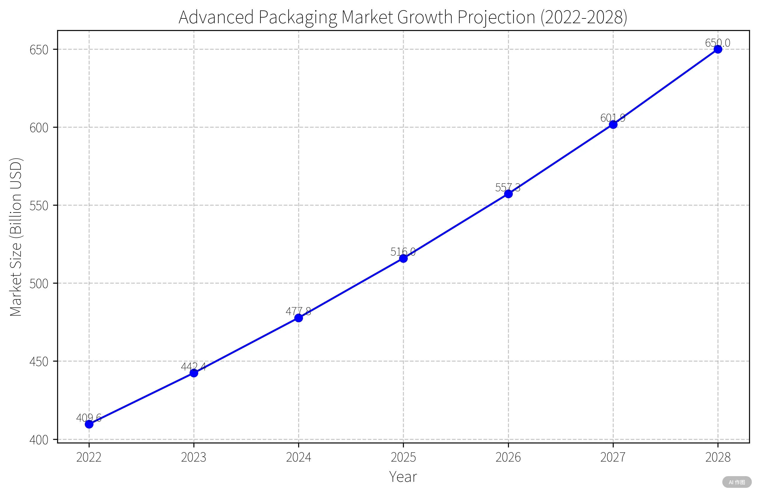
การคาดการณ์ตลาด (yole développement):
8% CAGR ผ่าน 2028 →ตลาด $ 65B
ตอนนี้บรรจุภัณฑ์กำหนดประสิทธิภาพของระบบอย่างยิ่ง - ไกลเกินกว่าการป้องกันเพียงอย่างเดียว.
บทสรุป
จากสนาม 2.54 มม. ของ DIP ไปจนถึงรอยเท้า 0.6 มม. ของ X2SON, ความก้าวหน้าของบรรจุภัณฑ์ใหม่อย่างต่อเนื่อง. ทุกสมาร์ทโฟน Slim และอุปกรณ์ 5G นั้นขึ้นอยู่กับนวัตกรรมที่มองไม่เห็นเหล่านี้. ด้วยการคำนวณ AI และควอนตัมที่เกิดขึ้นใหม่, บรรจุภัณฑ์ชิปจะผลักดันขอบเขตระดับนาโนต่อไป.
*ถัดไปในซีรีส์:
เทคโนโลยี BGA/CSP/WLCSP
3D บรรจุภัณฑ์ & TSV Interconnects
วิทยาศาสตร์วัสดุบรรจุภัณฑ์ขั้นสูงวิทยาศาสตร์
คอยติดตาม!*
