
การปฏิวัติวัสดุที่เงียบสงบเปลี่ยนอุปกรณ์อิเล็กทรอนิกส์
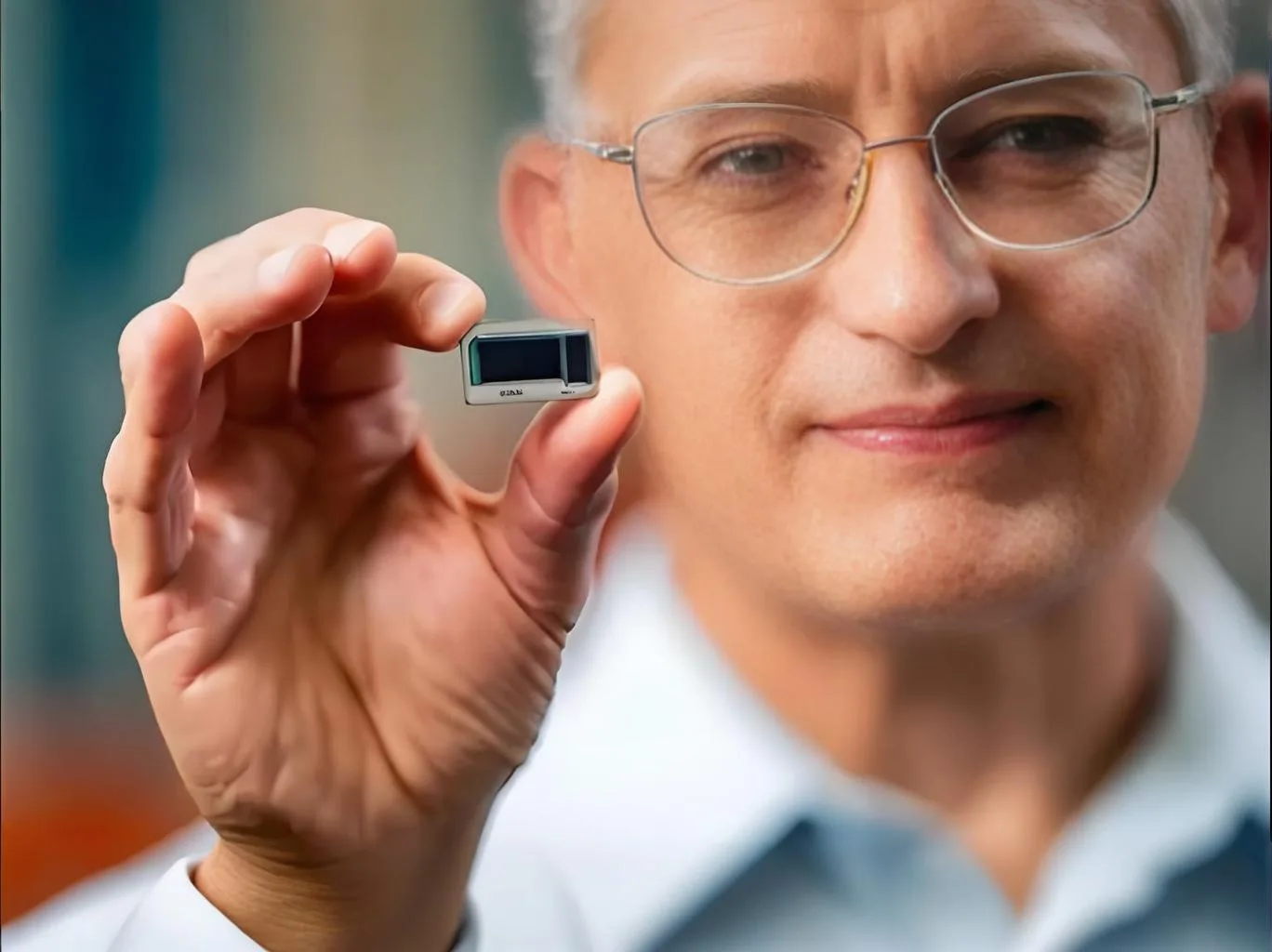
Intel's 2024 การเปิดตัว Global Global Glass บรรจุภัณฑ์ เทคโนโลยีจุดชนวนการเปลี่ยนแปลงแผ่นดินไหวในการผลิตเซมิคอนดักเตอร์. ที่ 2025 การประชุมสุดยอดอุตสาหกรรม Suzhou TGV, ผู้นำด้านเทคนิคจาก Intel, TSMC, และซัมซุงเห็นด้วย: “พื้นผิวแก้วจะขับเคลื่อนบรรจุภัณฑ์เซมิคอนดักเตอร์เข้าสู่ยุคโปร่งใส,’ ด้วยการเจาะตลาดเกินกว่า 50% ภายในห้าปี” การวิเคราะห์นี้สำรวจเหตุผลทางเทคโนโลยี, การเปลี่ยนแปลงห่วงโซ่อุตสาหกรรม, และผลกระทบสำหรับ พีซีบี อุตสาหกรรม.
1. ความเหนือกว่าทางเทคนิค: ทำไมพื้นผิวกระจกใหม่บรรจุภัณฑ์
1.1 การปกครองของทรัพย์สินทางกายภาพ
การวิเคราะห์เปรียบเทียบเผยให้เห็นพื้นผิวแก้ว’ ข้อได้เปรียบที่ล้นหลาม :
| พารามิเตอร์ | พื้นผิวอินทรีย์ | interposers ซิลิคอน | พื้นผิวกระจก |
|---|---|---|---|
| ค่าคงที่ไดอิเล็กตริก | 4.2-4.8 | 11.9 | 3.9 |
| สูญเสียแทนเจนต์ | 0.02-0.04 | 0.001-0.01 | 0.0001-0.001 |
| ซีทีอี (ppm/° C) | 16-18 | 2.6 | 3.2-7.5 (ปรับได้) |
| การนำความร้อน | 0.2-0.3 | 150 | 1.1 |
| ความขรุขระ | 0.5-1.0 μm | 0.05 μm | <0.01 μm |
(แหล่งที่มา: กระดาษสีขาวของ Intel, ห้องปฏิบัติการวัสดุ Corning)
การวิเคราะห์สมการการสูญเสียสัญญาณ
การลดทอน (อัน) หมายถึง:

ด้วยε'≈3.9และε”≈0.001สำหรับพื้นผิวแก้ว, ความถี่สูง (100กิกะเฮิรตซ์) การสูญเสียลดลงโดย 67% กับพื้นผิวอินทรีย์ (E'4.5, อี”≈0.03).
1.2 การเพิ่มความหนาแน่นแบบทวีคูณ
GB200 GPU ของ Nvidia แสดงให้เห็น 50%+ การเพิ่มจำนวนตายโดยใช้สารตั้งต้นแก้ว, บรรลุความหนาแน่นของการเดินสาย5μm/5μmผ่าน:
-
ความเรียบระดับอะตอม (<0.01ความขรุขระμm)
-
การจับคู่ CTE ที่ปรับได้ (3ppm/° C)
-
เสถียรภาพทางกล (700warpage แผง× 700 มม. <50μm)
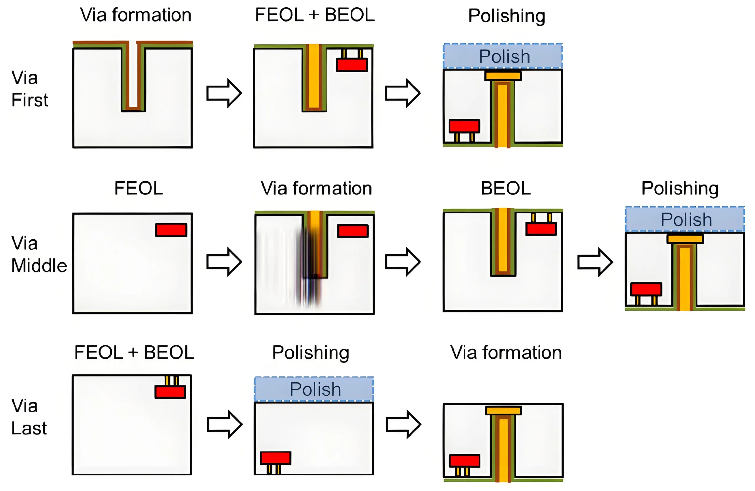
2. ประมวลผลนวัตกรรม: เทคโนโลยี TGV อุตสาหกรรม
2.1 ความก้าวหน้าในการผลิตผ่านแว่นตา-เวีย
การปรับเปลี่ยนเลเซอร์ของ Titanrise Tech สำเร็จ 8,000 Vias/Sec ที่ความแม่นยำ±5μm (3อัน), 160×เร็วกว่าวิธีการทั่วไป. ขั้นตอนสำคัญ:
-
การดัดแปลงเลเซอร์ Picosecond: สร้างโซนที่มีการเปลี่ยนแปลงในระดับไมครอน
-
การแกะสลัก HF: บรรลุผลสำเร็จ 100:1 อัตราส่วนภาพ
-
การทำให้เป็นโลหะ: PVD Sputtering + การชุบด้วยไฟฟ้า (>15การยึดเกาะ MPA)
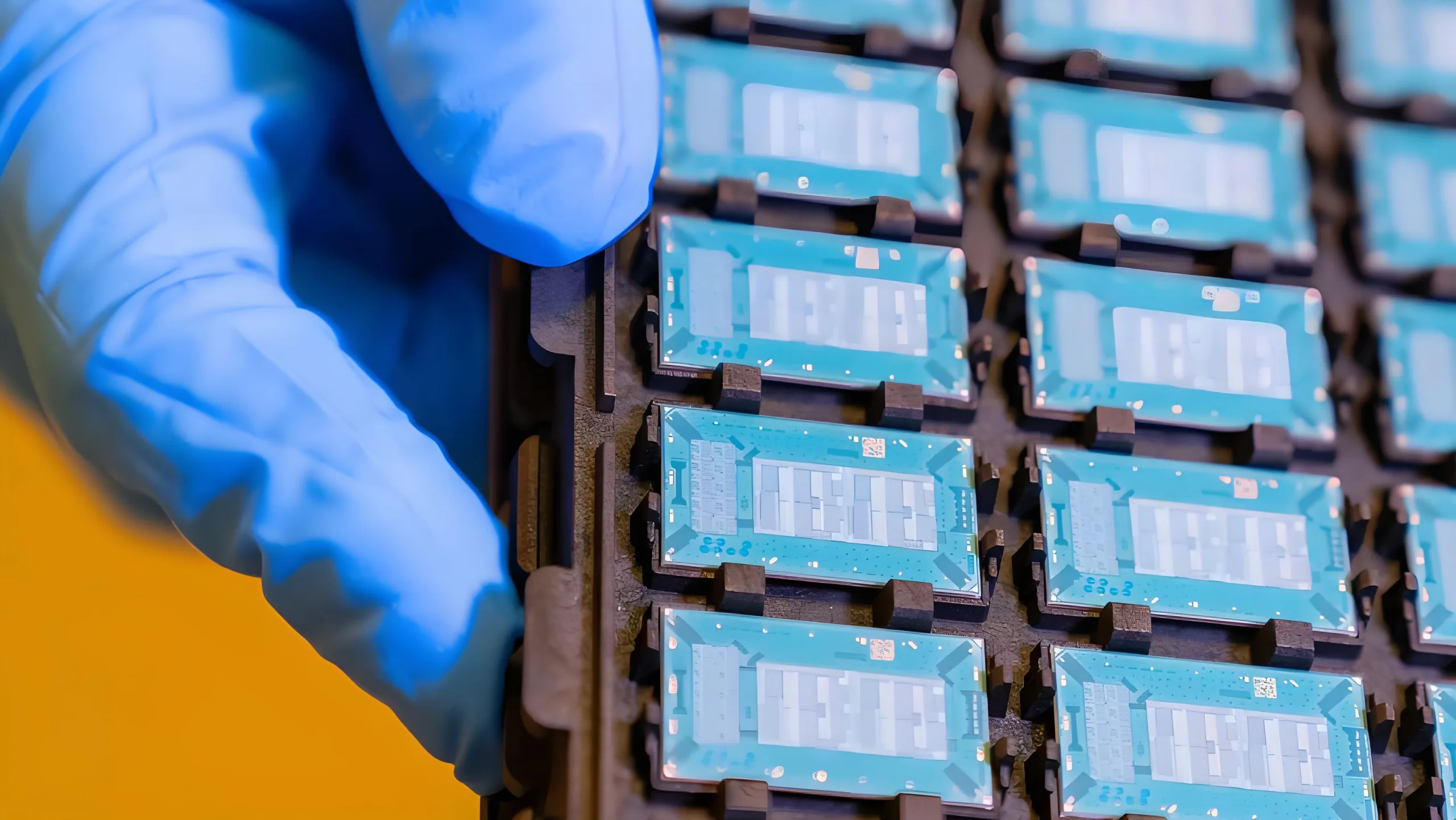
2.2 ความก้าวหน้าทางโลหะ
สี่เส้นทางทางเทคนิคที่อยู่การยึดเกาะกระจก:
-
ด้วยไฟฟ้าด้วย + การแกะสลักด้วยไมโคร (AKM Solutions)
-
Nano-Ag Paste + lt sintering (สิทธิบัตร Wintech)
-
การปลูกถ่ายอวัยวะในพลาสมา (เทคโนโลยี IME-CAS)
-
pvd ti/กับสแต็ก (Titanrise Standard)
ในหมู่พวกเขา, UGPCB ได้ลงทุนอย่างมากในการแนะนำอุปกรณ์ DEP600, ซึ่งใช้เทคโนโลยีสปัตเตอร์อัตราส่วนที่สูง, การบรรลุเป้าหมาย 95% ความครอบคลุม 10:1 โพรไฟล์, ด้วยความต้านทานโลหะน้อยกว่า 2.5 μΩ· cm, ถึงระดับนำในระดับสากล.
3. ภูมิทัศน์อุตสาหกรรม: การแข่งขันระดับโลกทวีความรุนแรงมากขึ้น
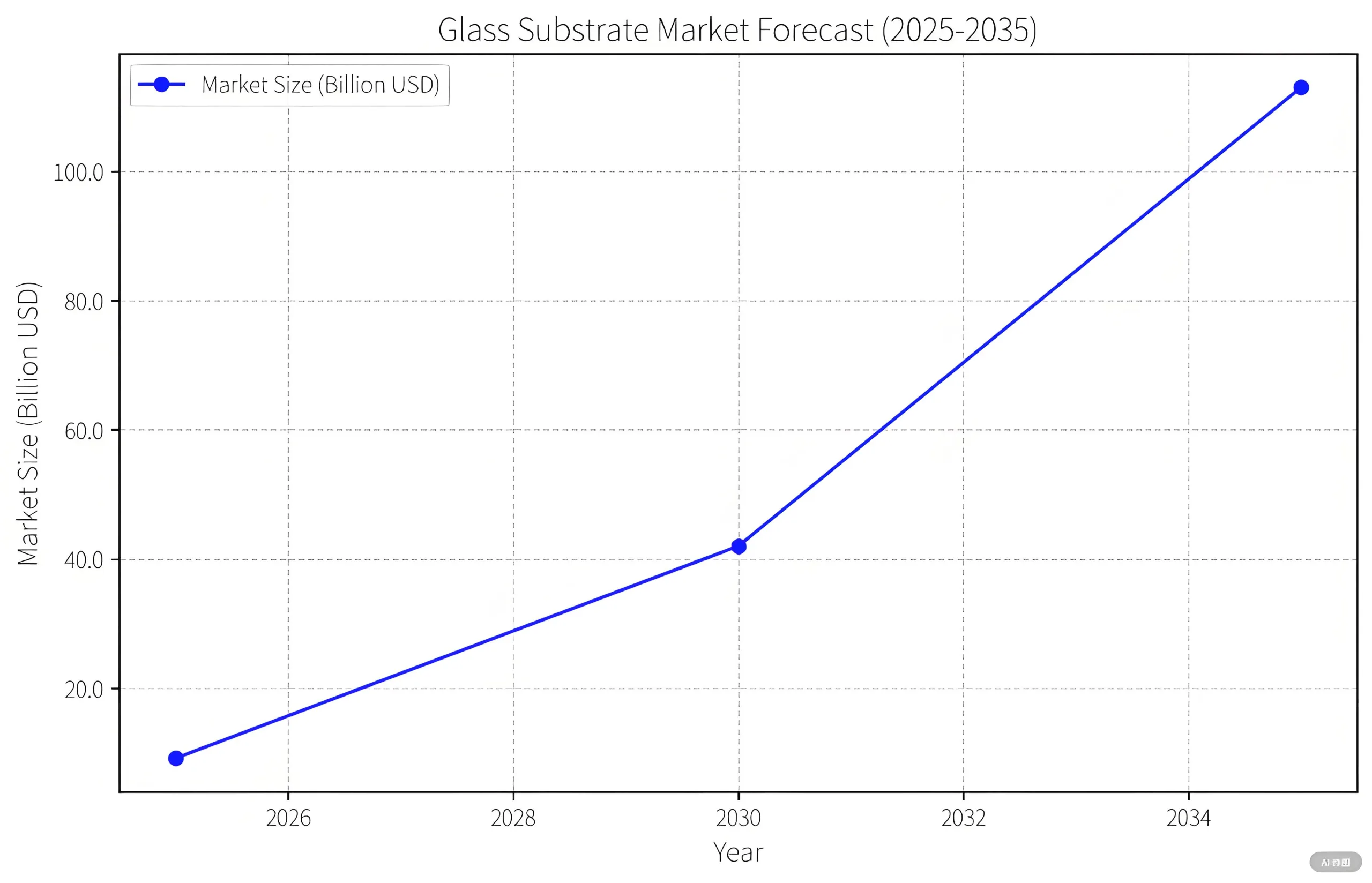
3.1 การคาดการณ์การเติบโตของตลาด
Prismark คาดการณ์การขยายตัวของระเบิด:
-
2025: $916ม. (พื้นผิว TGV)
-
2030: $4.2ข (แอปพลิเคชันเต็มรูปแบบ)
-
2035: $11.3ข (ระบบนิเวศทั้งหมด)
3.2 การแข่งขันด้านเทคโนโลยีทางการเมือง
-
สหรัฐอเมริกา: มาตรฐาน Intel + Corning Supply Dominance
-
เกาหลี: Samsung “พันธมิตรแก้ว” + กอง 9 ชั้นของ SKC
-
จีน: การผลิตมวล Wintech/AKM + jfe 2026 การแปลเป็นภาษาท้องถิ่น
4. ความท้าทาย & การแก้ปัญหา: อุปสรรคในเชิงพาณิชย์
4.1 เส้นทางการลดต้นทุน
ปัจจุบัน 3-5 ×ค่าใช้จ่ายพรีเมี่ยมเทียบกับพื้นผิวแบบดั้งเดิมจะลดลงผ่าน:
-
85% แผงขนาดใหญ่ (>2ตารางเมตร) การใช้ประโยชน์
-
90% การลดต้นทุนการขุดด้วยเลเซอร์
-
การปรับปรุงผลผลิตโลหะ (60%→ 92%)
4.2 การรับรองความน่าเชื่อถือ
ต้องใช้มาตรฐานใหม่:
-
การปั่นจักรยานความร้อน (-55° C - 2550 ° C, 1,000 รอบ)
-
อายุการใช้งาน (MTTF >10⁷ชั่วโมง @ jep154)
-
เสถียรภาพความถี่สูง (<0.5db/cm @100GHz)
5. ผลกระทบของอุตสาหกรรม PCB: ภัยคุกคามเทียบกับโอกาส
5.1 การหยุดชะงักของตลาด
-
30% HDI/พื้นผิว ความเสี่ยงทดแทน
-
ลูกผสม (แก้ว+เรซิน) โอกาสของสารตั้งต้น
5.2 การทำงานร่วมกันของเทคโนโลยี
-
Picosecond Laser Drilling ใช้
-
เพิ่ม PVD HDI ติดตามความแม่นยำ
-
การตรวจสอบด้วยแสง <0.1ความละเอียดμm
บทสรุป: พื้นผิวโปร่งใส, ฟิวเจอร์สทึบแสง
ตอนนี้จีนเป็นผู้นำภาค TGV ที่สำคัญ (อุปกรณ์, การทดสอบ, วัสดุ). ดังที่ Pat Gelsinger ของ Intel: “นวัตกรรมวัสดุกลายเป็นกฎหมายของมัวร์ใหม่ที่เครื่องชั่งอะตอม” การปฏิวัติที่ขับเคลื่อนด้วยแก้วนี้อาจปลดล็อกเส้นโค้งการเติบโตครั้งที่สองของเซมิคอนดักเตอร์เซมิคอนดักเตอร์.
