
ความก้าวหน้าทางเทคโนโลยีบรรจุภัณฑ์ทุกประการจะกำหนดขอบเขตทางกายภาพของอุปกรณ์อิเล็กทรอนิกส์ใหม่.
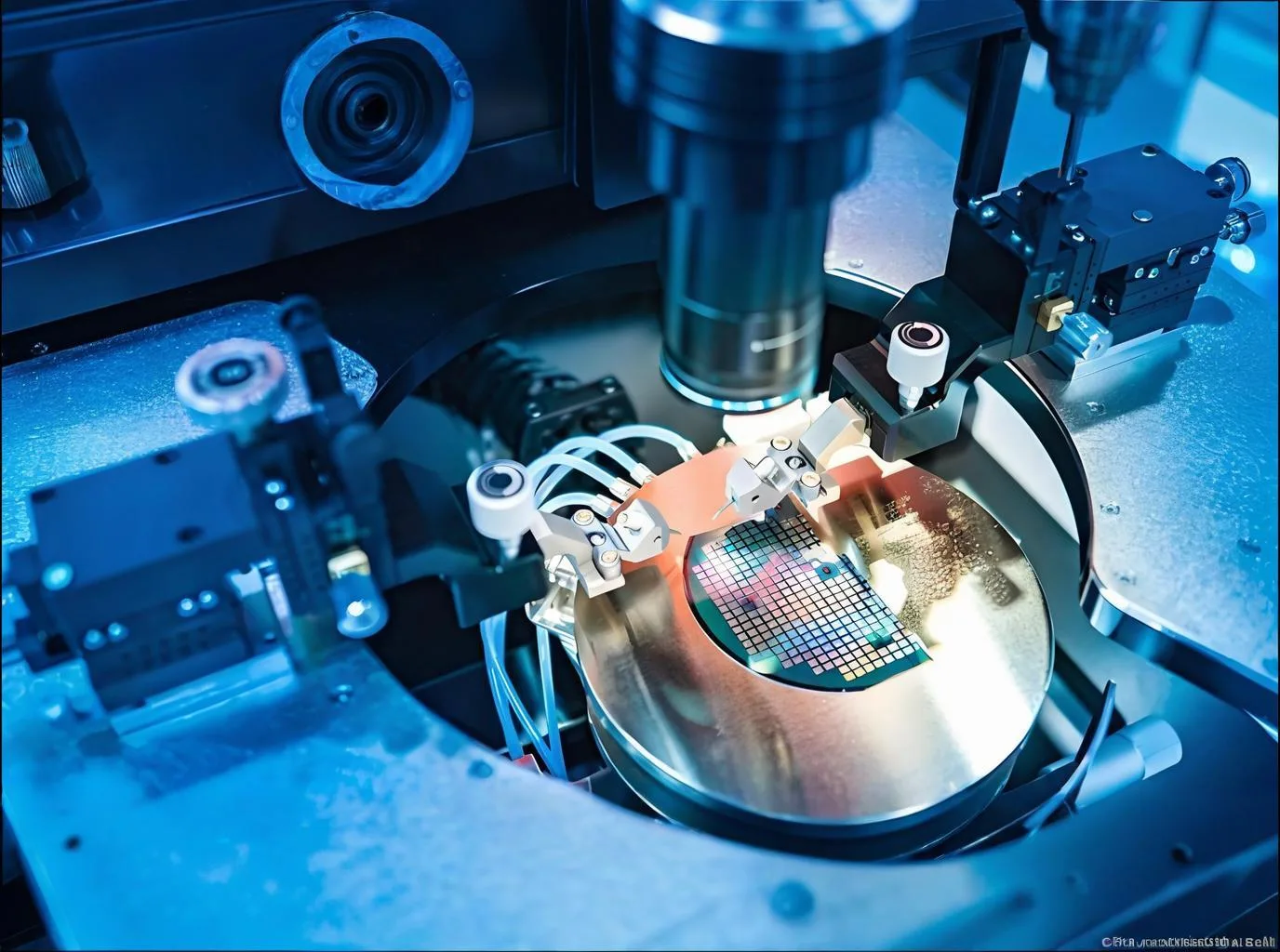
ในสัปดาห์ที่ผ่านมา วิวัฒนาการของบรรจุภัณฑ์แบบชิป: จาก DIP สู่ X2SON – การย่อส่วนเปลี่ยนโฉมอุปกรณ์อิเล็กทรอนิกส์อย่างไร, เราสำรวจยุคของบรรจุภัณฑ์แบบรูทะลุ (จุ่ม) และวิธีการติดตั้งอุปกรณ์บนพื้นผิว (จู่โจม, การสังเกตการณ์, ลูกชาย) เริ่มต้นการย่อขนาดอุปกรณ์. ในขณะที่เทคโนโลยีเหล่านี้วางรากฐานบรรจุภัณฑ์ที่ทันสมัย, ที่ การปฏิวัติการย่อขนาด ดำเนินต่อไป. วันนี้, เราตรวจสอบบรรจุภัณฑ์ที่มีความหนาแน่นสูงกว่า—ตั้งแต่แบบสี่แบนไปจนถึง CSP ระดับเวเฟอร์—และผลกระทบต่อแพ็คเกจเหล่านั้น การออกแบบ PCB ขีดจำกัด.
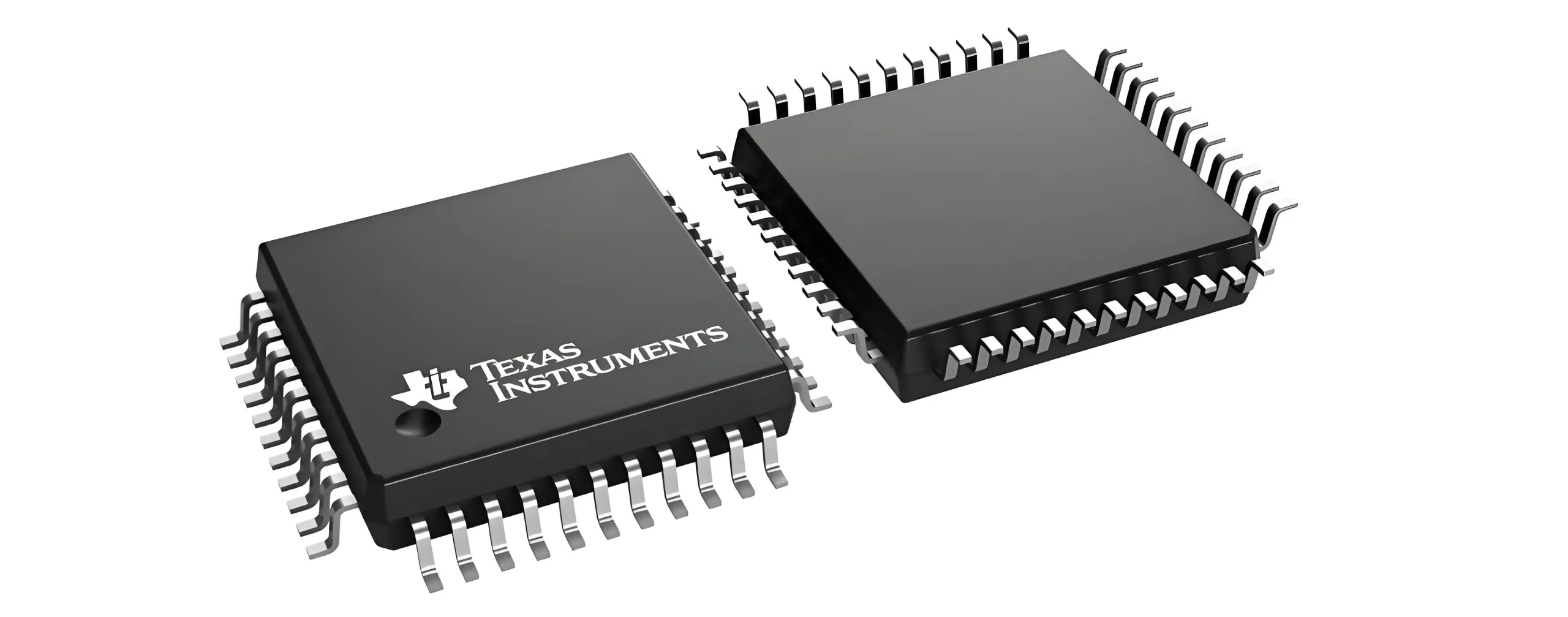
แพ็คเกจ Quad-Flat: สมดุลความหนาแน่นของอวกาศ
แพ็คเกจสี่แบน (MF, บมจ./คิวเอฟเจ, qfn) แสดงถึงวิวัฒนาการที่สำคัญไปสู่ความหนาแน่นของ I/O ที่สูงขึ้นโดยการใช้ขอบของแพ็คเกจทั้งสี่.
MF: ผู้บุกเบิกความหนาแน่นปีกนางนวล
MF (แพ็คเกจสี่แบน) คุณสมบัติที่โดดเด่น “ปีกนางนวล” (รูปตัว L) นำไปสู่การขยายจากทุกด้าน. ของมัน พินพิน (0.4มม./0.5มม./0.65มม) สั่งการ การกำหนดเส้นทาง PCB ความหนาแน่นและความแม่นยำในการบัดกรี.
ตัวแปร QFP:
-
ขนาด/ความหนา: LQFP (โปรไฟล์ต่ำ), ทีคิวเอฟพี (บาง), วีคิวเอฟพี (บางมาก)
-
วัสดุ: PQFP (พลาสติก), MQFP (โลหะ)
-
ปรับปรุงความร้อน: กองบัญชาการกองบัญชาการ, HLQFP, HTQFP, HVQFP
-
การป้องกัน: Bqfp (กันชน—แผ่นปิดมุมป้องกันไม่ให้สายงอ)
การจัดการระบายความร้อนเป็นสิ่งสำคัญ. สูตรต้านทานความร้อนแบบแยกต่อสิ่งแวดล้อม θja = (ทีจ-ตา)/P (ที่ไหน ทีจ= อุณหภูมิทางแยก, เผชิญหน้า= อุณหภูมิโดยรอบ, P=พลัง) ควบคุมการออกแบบการกระจายความร้อน.
บมจ./คิวเอฟเจ: ความมั่นคงผ่าน J-Leads
บมจ (ผู้ให้บริการชิปพลาสติกตะกั่ว) หรือคิวเอฟเจ (Quad Flat J-ลีด) ใช้สายวัดรูปตัว J ที่โค้งงอลงเพื่อความเสถียรทางกลต่อแรงสั่นสะเทือน/ความเครียดจากความร้อน.
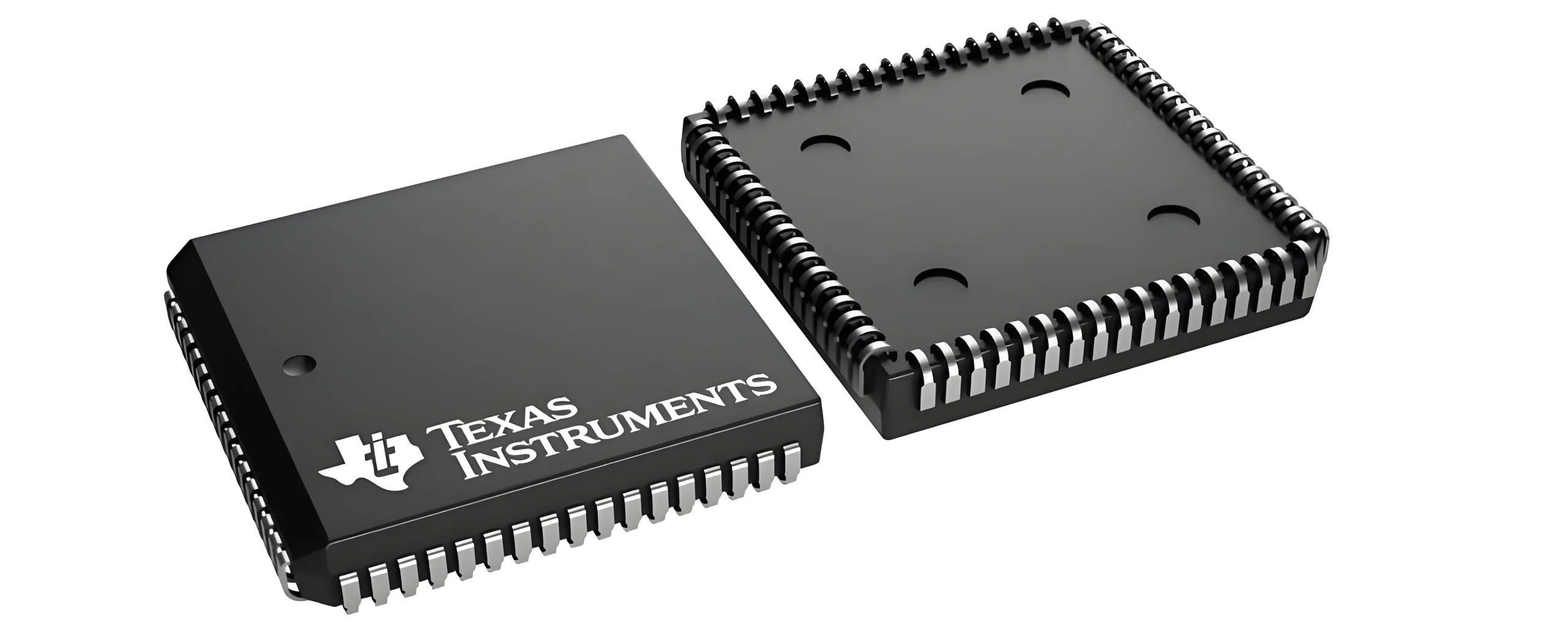
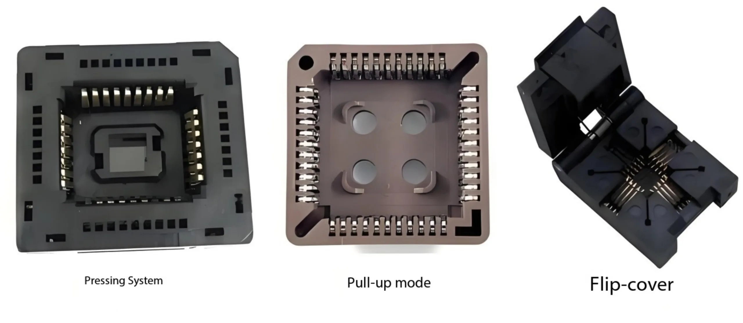
ข้อได้เปรียบด้านมาตรฐาน: ความเข้ากันได้สูงของ PLCC/QFJ กับซ็อกเก็ตทดสอบสากลทำให้การทดสอบการผลิตมีความคล่องตัว. แม้ว่า QFJ จะมีความแม่นยำทางเทคนิคก็ตาม, “บมจ” ยังคงเป็นที่ต้องการของอุตสาหกรรม.
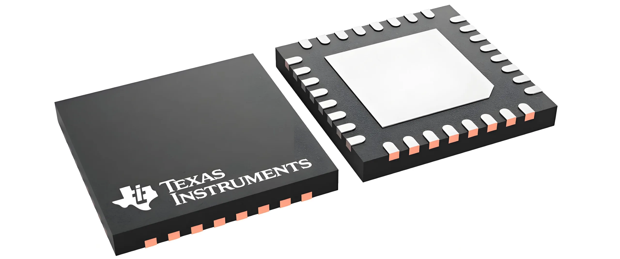
qfn: ความก้าวหน้าของการย่อส่วนแบบไร้สารตะกั่ว
qfn (Quad Flat ไม่มีสารตะกั่ว) กำจัดโอกาสในการขายภายนอก, เชื่อมต่อผ่าน:
-
สัมผัสแผ่น (อีพี): เส้นทางระบายความร้อนโดยตรงไปยัง พีซีบี ทองแดง
-
สีข้างที่เปียกได้: แผ่นบัดกรีติดผนังด้านข้าง
ข้อดีที่สำคัญ:
-
กะทัดรัดเป็นพิเศษ: 40% เล็กกว่า QFP
-
ความเหนือกว่าทางไฟฟ้า: เส้นทางที่สั้นกว่าจะลดการเหนี่ยวนำของปรสิต (ลิตร หยาบคาย ไมโครลิตร/วัตต์)
-
ประสิทธิภาพเชิงความร้อน: θja ต่ำกว่าเทียบกับ. QFP ขนาดเดียวกัน
วิวัฒนาการความหนา: LQFN → UQFN → VQFN → WQFN → X1QFN → X2QFN. แอลซีซี (แอล.ซี.ซี./แอล.ซี.ซี) คือเซรามิก/พลาสติกไร้สารตะกั่ว.
แพ็คเกจอาร์เรย์: ปฏิวัติขีดจำกัดความหนาแน่น
เมื่อ quad-flat ถึงขีดจำกัด I/O, แพ็คเกจอาร์เรย์ (แอลจีเอ, BGA) เปิดใช้งานความหนาแน่นของการเชื่อมต่อระหว่างกัน 2D.
แอลจีเอ: การเชื่อมต่อแบบยืดหยุ่นที่แม่นยำ
แอลจีเอ (อาร์เรย์กริดที่ดิน) ใช้หน้าสัมผัสโลหะที่จัดตำแหน่งอย่างแม่นยำ (เช่น, แอลจีเอ775: 775 ผู้ติดต่อ) ผสมพันธุ์กับหมุดซ็อกเก็ต.
ค่าหลัก:
-
ความสามารถในการเสียบปลั๊ก: การอัพเกรด/บำรุงรักษา CPU
-
ความเหนี่ยวนำต่ำ: เส้นทางสัญญาณสั้น
-
ความน่าเชื่อถือสูง: เหมาะสำหรับซีพียู (อินเทล/เอเอ็มดี)
ข้อจำกัด: ต้นทุน/ขนาดซ็อกเก็ตที่สูงเอื้อต่อ BGA ในอุปกรณ์ขนาดกะทัดรัด. บันทึก: LGA สามารถบัดกรี direct-SMT ได้.
BGA: การครอบงำบอลประสาน
BGA (อาร์เรย์กริดบอล) เชื่อมต่อผ่านเมทริกซ์บอลประสาน. สนามบอล (0.3–1.0mm; <0.2มม. สำหรับ FBGA) เป็นสิ่งสำคัญ.
ข้อดีการเปลี่ยนแปลง:
-
ความหนาแน่นสูง: >1,000 ฉัน/พวกเรา (VS. QFP ~300)
-
ประหยัดพื้นที่: 30%+ การลดพื้นที่เทียบกับ. MF
-
ไฟฟ้า/ความร้อน: ความล่าช้าของสัญญาณต่ำ; ลูกบอลนำความร้อน
-
การจัดตำแหน่งตนเอง: การประกอบตัวช่วยแรงตึงผิว
ครอบครัวบีจีเอ:
-
วัสดุ: พีบีก้า (พลาสติก), CBGA/CABGA (เซรามิค)
-
ขนาด/ระยะพิทช์: nFBGA/FBGA (ปรับระดับเสียง), ไทนี่บกา, DSBGA/WCSP (ขนาดแม่พิมพ์), แอลเอฟบีจีเอ/วีเอฟบีจีเอ (บาง)
-
การรวมเข้าด้วยกัน:
-
เอฟซีบีจีเอ (พลิกชิป): การเชื่อมต่อแบบดายกับพื้นผิวโดยตรงผ่านไมโครบัมเปอร์
-
โผล่ (แพ็คเกจบนแพ็คเกจ): การวางซ้อนในแนวตั้ง (เช่น, ตรรกะ + หน่วยความจำ)
-
PG-WF2BGA: บรรจุภัณฑ์ระดับเวเฟอร์แบบพัดออก
-
ความท้าทาย: การตรวจเอ็กซ์เรย์ (แอ็กซี่), การทำงานซ้ำที่ซับซ้อน, การจับคู่ CTE วัสดุ PCB.
การเปรียบเทียบแพ็คเกจอาร์เรย์
| คุณสมบัติ | PGA (ปักหมุดอาร์เรย์กริด) | แอลจีเอ (อาร์เรย์กริดที่ดิน) | BGA (อาร์เรย์กริดบอล) |
|---|---|---|---|
| การเชื่อมต่อ | หมุดแข็ง | หน้าสัมผัสระนาบ | ลูกประสาน |
| จุดแข็งที่สำคัญ | ความน่าเชื่อถือของซ็อกเก็ต | ความหนาแน่น + เสียบปลั๊กได้ | ความหนาแน่นสูงสุด/ขนาดนาที |
| ความล่าช้าของสัญญาณ | สูงสุด | ปานกลาง | ต่ำสุด |
| การใช้งาน | CPU รุ่นเก่า/อุตสาหกรรม | ซีพียูเดสก์ท็อป/เซิร์ฟเวอร์ | อุปกรณ์เคลื่อนที่/GPU/SoC |
| พื้นที่พีซีบี | ใหญ่ | ปานกลาง | กะทัดรัด |
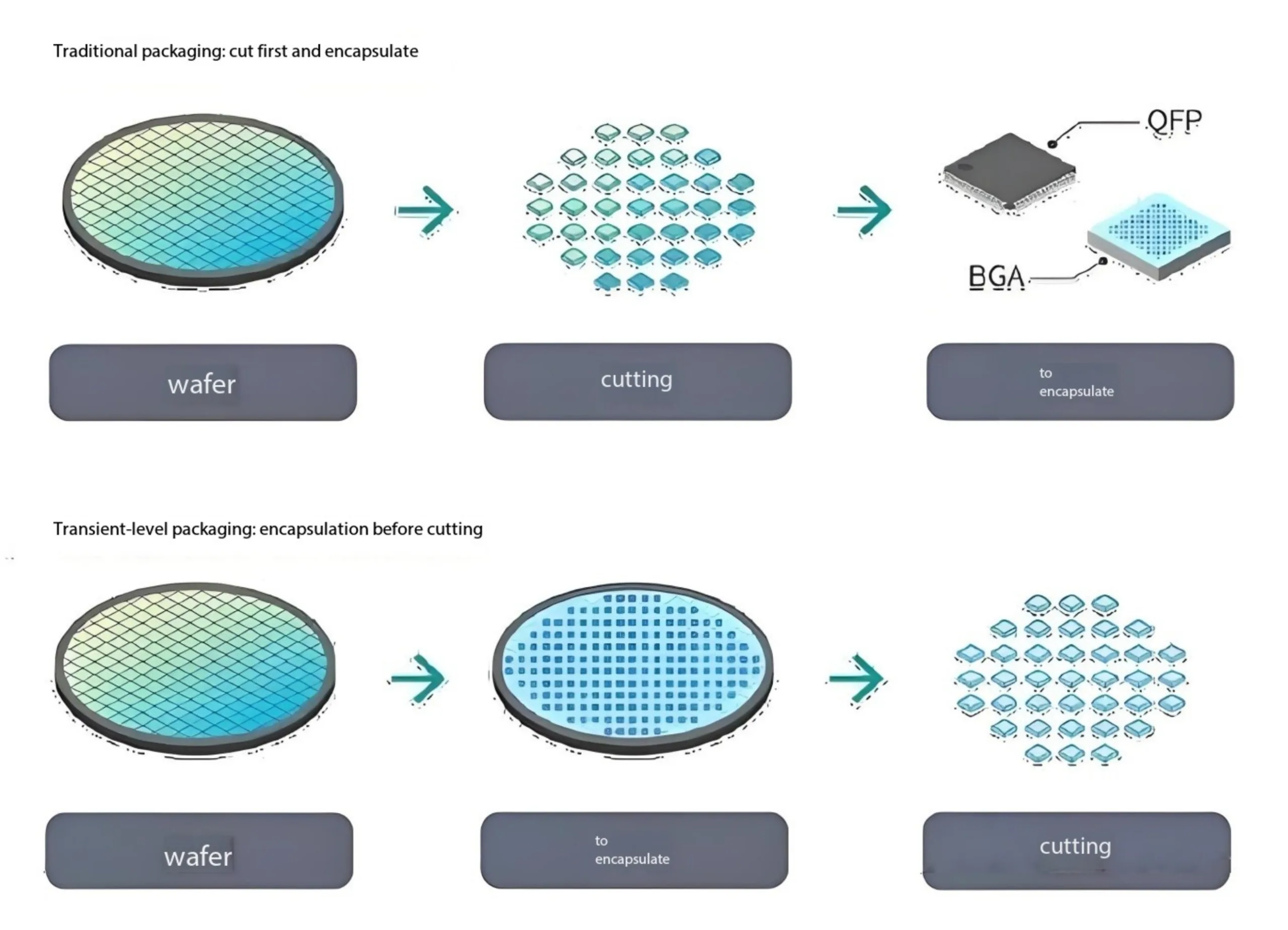
ชิปขนาด & แพ็คเกจระดับเวเฟอร์: เข้าใกล้ขีดจำกัดทางกายภาพ
CSP: กำหนดขอบเขตขนาดใหม่
CSP (แพ็คเกจเครื่องชั่งชิป) ตัวชี้วัดที่สำคัญ: ขนาดบรรจุภัณฑ์ ≤ 1.2× ขนาดแม่พิมพ์ (VS. 2–5× สำหรับแบบดั้งเดิม). BGA ย่อส่วนโดยพื้นฐานแล้ว (FBGA/VFBGA) ด้วยระดับเสียงที่ละเอียดยิ่งขึ้น (0.2–0.5มม).
ค่า: การย่อขนาดขั้นสูงสุดสำหรับอุปกรณ์สวมใส่/เซ็นเซอร์.
WlcSp: การปฏิวัติระดับเวเฟอร์
การบรรจุ WLCSP/Wafer-Level เสร็จสิ้นทุกขั้นตอน (อาร์ดีแอล, การตีลูก) บนเวเฟอร์ก่อนหั่นเป็นลูกเต๋า.
ข้อดีที่ก่อกวน:
-
ขนาดที่เล็กที่สุด: ➤ ขนาดแม่พิมพ์
-
การลดต้นทุน: 30-50% ถูกกว่า (ไม่มีสารตั้งต้น/การขึ้นรูป)
-
ประสิทธิภาพสูงสุด: การเชื่อมต่อที่สั้นที่สุด, ปรสิตต่ำสุด
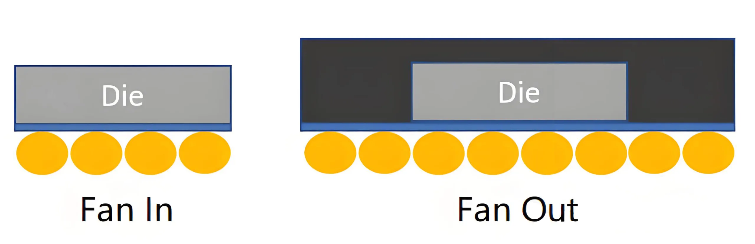
ประเภท WLCSP:
-
แฟนอิน WLCSP:
-
ลูกบอลภายในพื้นที่ตาย
-
ขนาดบรรจุภัณฑ์ = ขนาดแม่พิมพ์
-
ต้นทุนต่ำสำหรับเซ็นเซอร์/PMIC
-
-
WLCSP แบบกระจายออก (เช่น, ข้อมูลทีเอสเอ็มซี, ซัมซุง FO-PLP):
-
ลูกบอลขยายออกไปเกินกว่าจะตาย
-
ขนาดบรรจุภัณฑ์ > ขนาดตาย
-
ความหนาแน่นของ I/O ที่สูงขึ้น, การรวมหลายชิป
-
สำหรับโมดูล SoCs/RF ระดับพรีเมียม
-
รหัสภาพ: ซิลิกอนที่ไม่มีการห่อหุ้ม (VS. DFN ที่ขึ้นรูปด้วยเรซิน).
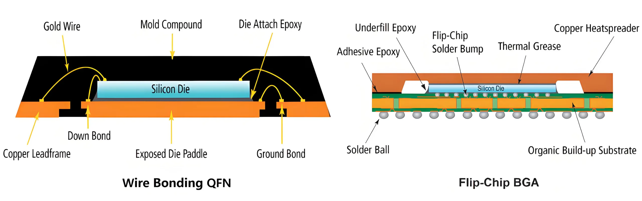
สัณฐานวิทยาของบรรจุภัณฑ์ & เทคนิคการติด
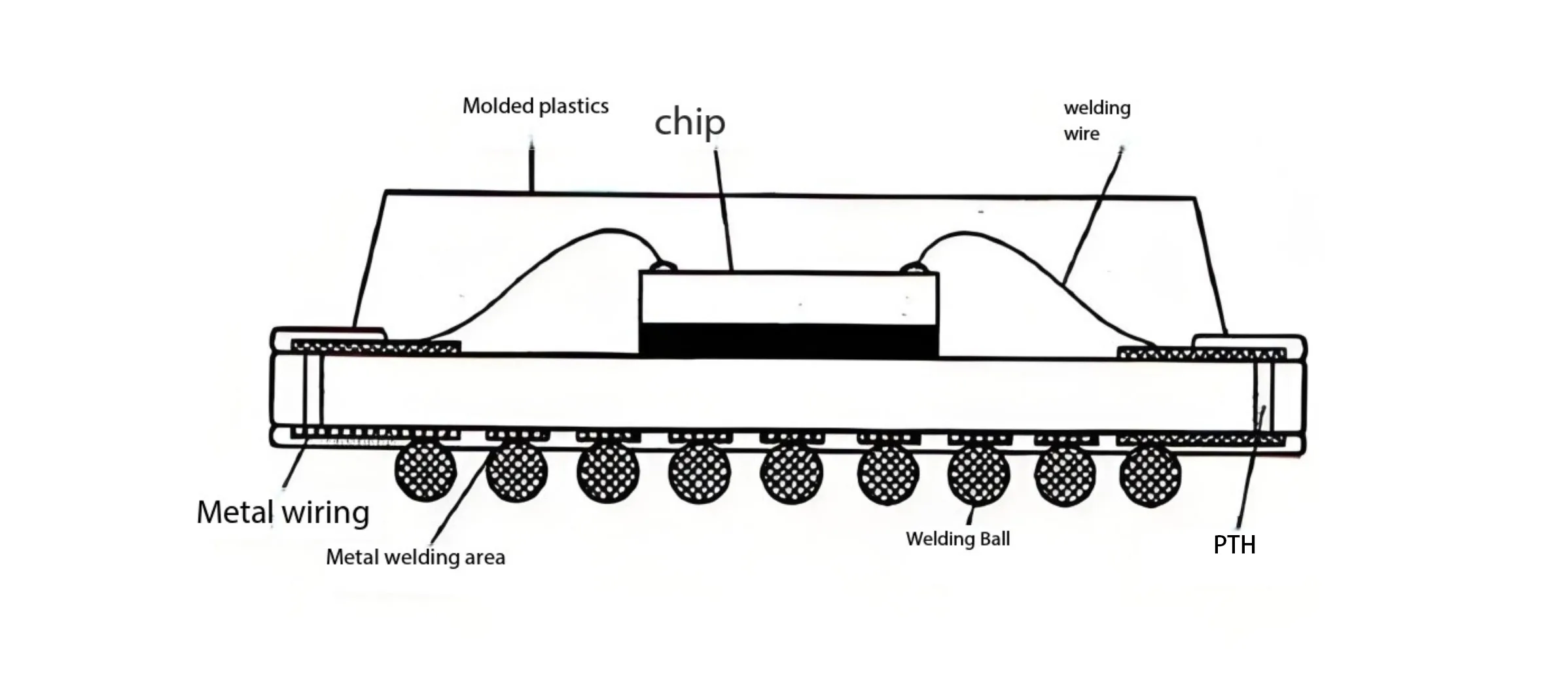
แบบฟอร์มแพ็คเกจภายนอก (QFP/BGA/WLCSP) และพันธะภายในนั้นเชื่อมโยงกันภายใน:
-
การติดลวด:
-
เป็นผู้ใหญ่, ต้นทุนต่ำ
-
ครอง QFP/QFN/BGA ระดับกลาง
-
มี/มีสายไฟ; I/O ปานกลาง
-
-
พลิกชิป:
-
ดายแนบคว่ำหน้าด้วยไมโครบัม
-
การเชื่อมต่อที่สั้นที่สุด, ความเหนี่ยวนำต่ำสุด
-
จำเป็นสำหรับ FCBGA/WLCSP/CSP ประสิทธิภาพสูง
-
บทสรุป & พรมแดนในอนาคต
จาก QFP ไปจนถึง LGA/BGA และสุดท้ายคือ CSP/WLCSP, วิวัฒนาการของบรรจุภัณฑ์ชิปคือก พงศาวดารของการบีบอัดพื้นที่, ประสิทธิภาพเพิ่มขึ้น, และการเพิ่มประสิทธิภาพต้นทุน. การย่อส่วนแบบก้าวกระโดดแต่ละครั้งจะปรับโฉมการออกแบบ PCB ใหม่—ขับร่องรอยที่ละเอียดยิ่งขึ้น, หลายชั้น HDI, และวัสดุขั้นสูง.
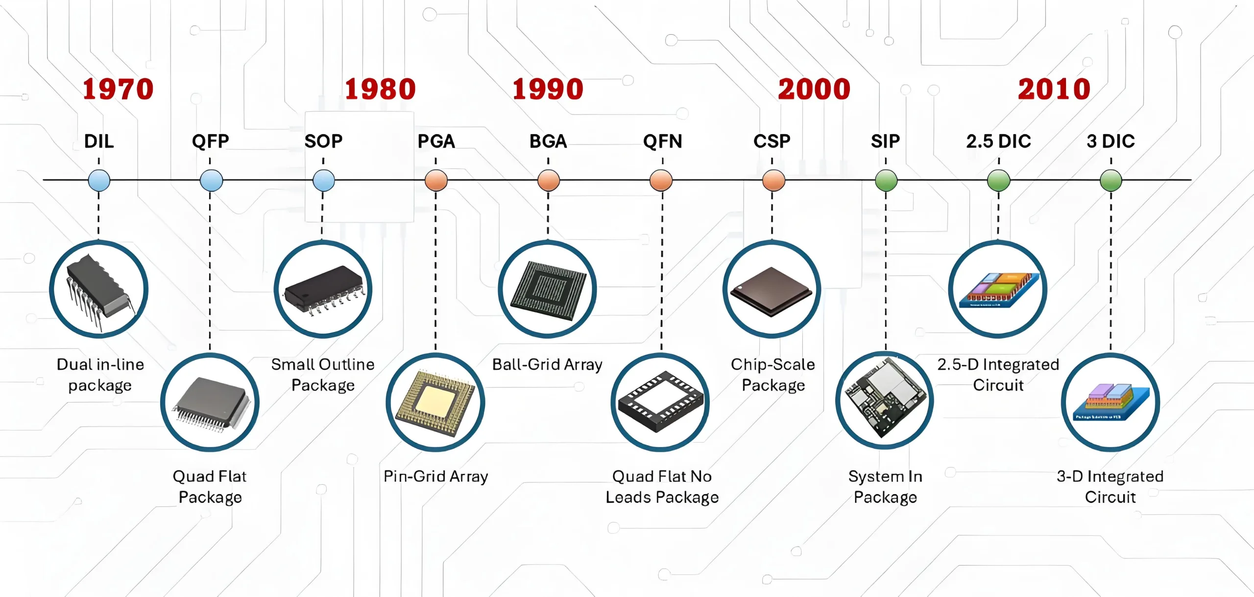
ชายแดนถัดไป: เทคโนโลยีเช่น TSV (ผ่านซิลิคอนผ่าน), จิบ (ระบบในแพ็คเกจ), และ 2.5D/3D IC ช่วยให้สามารถบูรณาการ 3D Heterogeneous ได้แล้ว, ผลักดันการออกแบบ PCB ไปสู่มิติใหม่ รับชมได้ในบทความถัดไปของเรา.
เมื่อทรานซิสเตอร์หนึ่งพันล้านตัวบรรจุอยู่ในบรรจุภัณฑ์ขนาดเท่าเม็ดทราย, การต่อสู้ทางวิศวกรรมอิเล็กทรอนิกส์ในระดับโมเลกุล.

Thanks for sharing the information with us.
whoah this blog is magnificent i really like reading your articles. Keep up the good paintings! You recognize, many people are searching round for this info, you can help them greatly.