
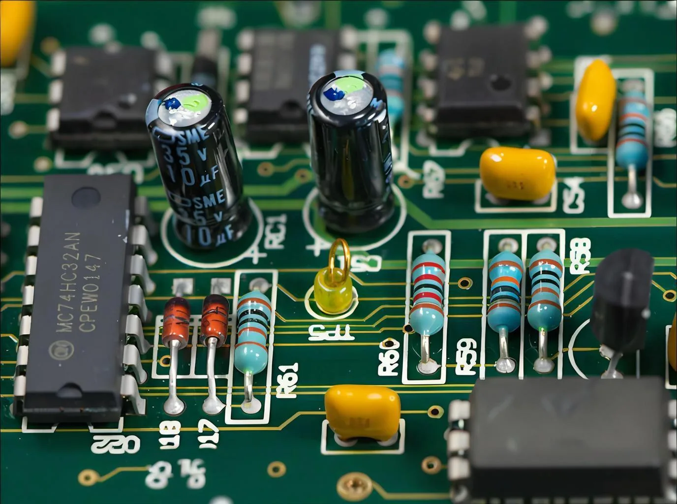
|Look at a smartphone motherboard. A dense maze of components and traces unfolds before you. The tiny white silkscreen characters act as a crucial map, guiding engineers through this electronic labyrinth.
On a smartwatch พีซีบี, a character as small as 0.2mm remains legible. A QR code on an automotive control board stores the board’s entire lifecycle data, from production to maintenance. Temperature-sensitive indicators on industrial equipment PCBs change color automatically to warn of overheating. These seemingly simple printed markings are driving electronics manufacturing toward greater intelligence and precision.
01 Fundamentals and Standards of PCB Silkscreen Printing
PCB silkscreen printing, or legend printing, is far more than just “printing a few letters.” It is a comprehensive process integrating electronic engineering, วัสดุศาสตร์, and precision manufacturing. These characters serve as the circuit board’s “identity” และ “operational guide,” performing core functions like component identification, polarity indication, test point marking, and version control.
Key design parameters directly impact production yield. According to relevant มาตรฐาน IPC, character line width and height should be proportional. For solid characters, the stroke width should not be less than 0.15mm, with a character height ≥0.75mm. For higher precision applications, a minimum stroke width of 0.1mm and a minimum character height of 0.8mm are achievable.
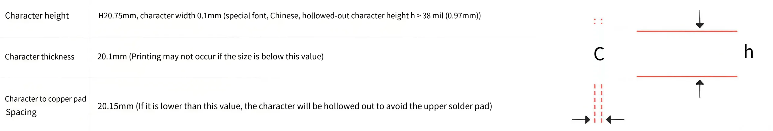
Equally critical is the clearance control between the silkscreen and solder pads, which directly affects subsequent SMT soldering คุณภาพ. Industry standards mandate a minimum distance of 0.15mm between silkscreen and pads, and a minimum 0.15mm gap between silkscreen lines themselves. When clearance falls below this parameter, overlapping silkscreen is typically removed from the pad area in engineering to prevent solder bridging and other แอสเซมบลี PCBA issues.
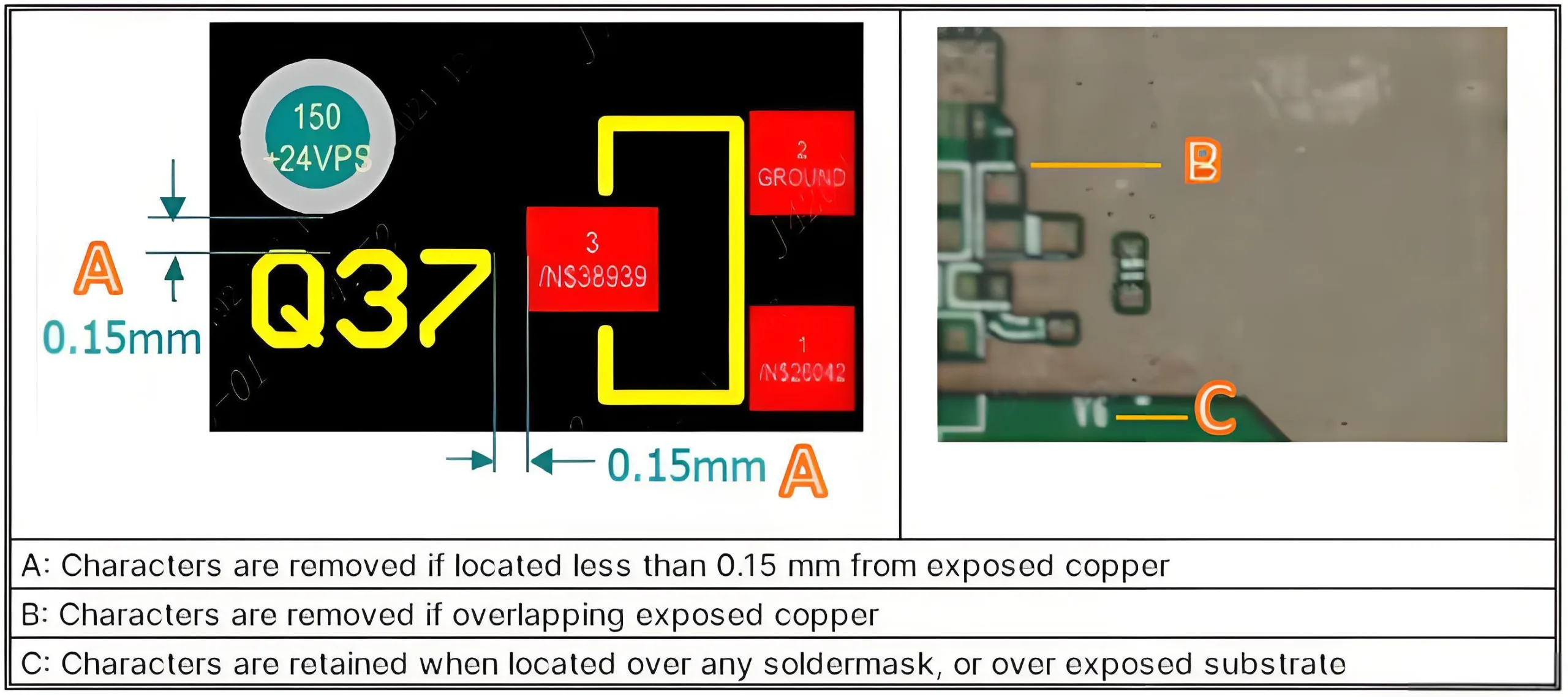
Another often-overlooked detail is silkscreen on copper surfaces. Characters placed on exposed copper, เลือดออก, or gold-plated surfaces are usually deleted due to vastly different adhesion properties compared to the base laminate. If required by the customer, this must be explicitly noted in the order and confirmed against the production panel.
02 The Evolutionary Path of PCB Silkscreen Printing Technology
PCB silkscreen technology has undergone a significant shift from traditional screen printing to digital inkjet printing. Traditional screen printing uses a stencil and mesh screen—hence the term “silkscreen.” While cost-effective for high-volume production, it faces limitations in precision and flexibility.
The advent of digital inkjet printing technology has revolutionized the process. This method uses digital inkjet heads to deposit functional inks directly onto the insulating substrate, forming patterns for etch resists, legends, มาสก์บัดกรี, and even circuits. Compared to traditional screen printing, digital inkjet offers clear advantages in process simplification, ประสิทธิภาพ, material/cost savings, and environmental friendliness.
The market size for digital inkjet printing in China’s PCB industry grew from $297 ล้านใน 2017 ถึง $1.065 พันล้านใน 2022, representing a remarkable compound annual growth rate (cagr) ของ 29.10%. Driven by advancements in 5ช, AI, and cloud computing, this market is projected to continue growing at a CAGR of 17.83% ในอีกห้าปีข้างหน้า.
03 Technological Innovations in Modern PCB Silkscreen Printing
Modern PCB silkscreen printing has evolved beyond simple identification into smart, functional, and eco-friendly applications.
Regarding การย่อขนาดเล็ก, เช่น การเชื่อมต่อระหว่างกันที่มีความหนาแน่นสูง (HDI) พีซีบี pitches shrink below 0.2mm, traditional characters become inadequate. Industry innovators now achieve ultra-fine characters of 8-12 mils (0.203-0.305มม) with line widths reduced to 3-4 mils (0.076-0.102มม). This requires high-mesh screens (600-800) paired with high-precision screen printers boasting positioning accuracy of ±0.01mm.
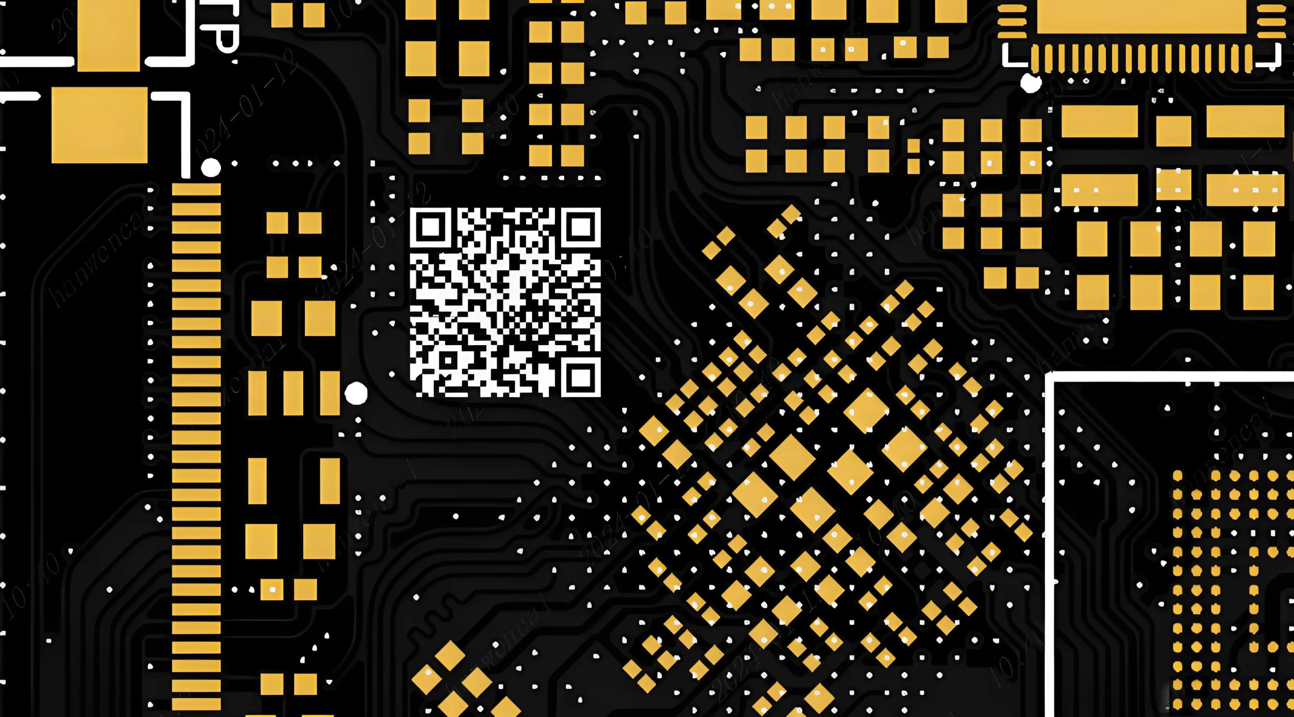
Smart silkscreen printing represents another breakthrough. By integrating miniature QR codes—as small as 2mm x 2mm—complete PCB lifecycle data can be embedded. With a scan speed of <0.5 seconds per board, traceability efficiency improves by up to 80%.
More advanced is “sensory silkscreen” using thermochromic ink. Temperature indicators printed with this ink change color when the PCB exceeds a set temperature, enabling monitoring without additional sensors.
Eco-friendly innovation is also crucial. Solvent-free inks utilizing 100% solid UV-curable formulas limit VOC emissions to ≤10mg/m³, while achieving adhesion strength ≥3.5N/cm and heat resistance exceeding 125°C. Bio-based inks, derived from plant resins instead of petroleum, offer biodegradation rates over 60% and are ideal for applications with stringent environmental requirements, such as medical devices.
04 Material Science Breakthroughs in PCB Printing Inks
The quality of silkscreen printing is heavily dependent on ink material performance. หมึกหน้ากากประสาน, a key material in การผลิต PCB, primarily consists of epoxy resin (50%), pigments/fillers (45%), and solvents/additives (5%).
Technically, high-quality inks require a flash point ≥95°C, a density of 1.8g/cm³, and must pass solder resistance tests (เช่น, 288°C for 10 seconds without blistering).
Controlling solder mask thickness is vital for quality. Industry standards typically specify a thickness range of 15-35μm. The solder mask dam (สะพาน) width must be adjusted based on copper weight: ≥0.08mm for copper ≤1oz and ≥0.12mm for copper ≥2oz.
Curing processes vary by application: UV-curable types suit automated mass production with energy doses of 800-1200 mJ/cm²; thermal-curable types use a three-stage temperature profile; photoimageable types offer the highest precision but require multiple steps like pre-bake, การรับสัมผัสเชื้อ, and development.
Recent material innovations include bio-based structural photo-curable copolymer inks developed in 2024, reducing reliance on petroleum-based materials while excelling in adhesion, ความแข็ง, ปณิธาน, and plating resistance.
05 Intelligence and Automation in PCB Silkscreen Printing
In modern PCB manufacturing facilities like UGPCB, silkscreen printing is fully integrated into intelligent production systems. Every circuit board’s history is traceable, enabling digital control from order entry to shipping.
Via 5G private networks, real-time equipment status and energy data are uploaded. The system automatically alerts for faults, improving response times by 50%. An intelligent tool management system preemptively warns of tool replacement needs, ensuring micron-level machining accuracy.
In quality inspection, Aoi scanners perform high-speed checks, flying probe testers provide precise diagnostics, and the automated production system monitors the entire流程 like a strict overseer. If chemical bath analysis shows anomalies, the system immediately halts production and initiates automatic replenishment, creating an intelligent quality control loop.
06 Future Trends and Outlook
PCB silkscreen printing is advancing toward higher integration, enhanced functionality, and superior sustainability. Multi-process integration is a clear trend, where silkscreen is no longer an isolated step but deeply integrated with solder mask application, circuit patterning, and assembly processes.
Software tools that automatically align solder mask openings with silkscreen clearance can reduce design conflicts from 10% ถึง 0.1%.
Silkscreen outlines can act as fiducials for SMT pick-and-place machine vision systems, achieving placement accuracy of ±0.03mm and reducing misplacement rates from 0.5% ถึง 0.1%. Printing assembly guidance graphics, like arrows and sequence numbers, can direct automated assembly robots, boosting efficiency by 20%.
In specialized fields like aerospace and medical PCBs, requirements are more stringent. High-temperature resistant inks must withstand over 180°C, with adhesion loss not exceeding 5% หลังจาก 2000 วงจรความร้อน. Medical PCBs employ “sterile ink + sterile curing” processes compliant with FDA 21 CFR Part 175, ensuring a sterility assurance level of ≤10 CFU per unit.
As devices trend toward miniaturization and higher performance, PCB character printing technology continues to innovate. From simple identification to today’s smart, interactive applications, this seemingly minor process carries the dual mission of precision and intelligence in electronics manufacturing. Those tiny markings on the board silently document each step forward in intelligent manufacturing.

Incredible! This blog looks just like my old one! It’s on a entirely different subject but it has pretty much the same page layout and design. Great choice of colors!