

ภาพรวมผลิตภัณฑ์ระดับมืออาชีพ: The 12-Layer High-Speed, PCB ความหนาแน่นสูง
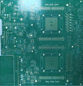
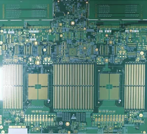
In the era of high-speed data transmission and complex system integration, conventional printed circuit boards (PCBS) fall short of meeting the performance demands of advanced electronics. ที่ 12-layer high-speed, PCB ความหนาแน่นสูง is the engineered solution. Featuring up to 12 precisely aligned conductive layers, it enables intricate interconnections and efficient signal transmission within a compact footprint, serving as the “ระบบประสาทส่วนกลาง” for high-end networking gear, data center servers, คอมพิวเตอร์ประสิทธิภาพสูง (HPC), and AI hardware.
As an expert ผู้ผลิต PCB และ ผู้จำหน่าย PCB, UGPCB leverages advanced processes to deliver reliable 12-ชั้น บอร์ด PCB การผลิต, ensuring your products maintain a competitive performance edge.
In-Depth Parameter Analysis: The Foundation of Performance
The capability of a high-quality แผงวงจรพิมพ์หลายชั้น is defined by its specifications. Below is an analysis of this product’s core parameters:
-
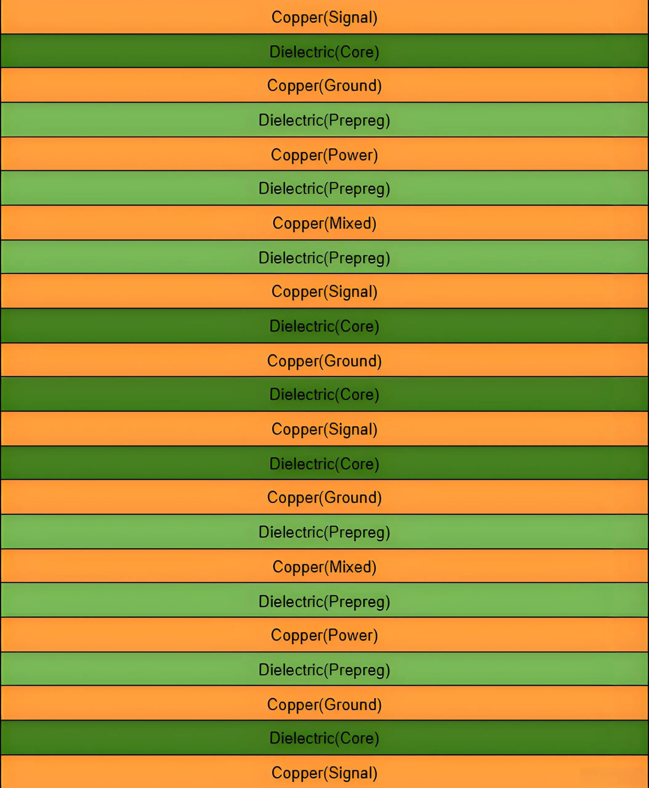
จำนวนเลเยอร์ & ซ้อนขึ้น: 12 ชั้น. นี้ multilayer PCB design offers superior signal integrity (และ), ความสมบูรณ์ของพลังงาน (PI), and EMC performance compared to boards with fewer layers. It allows for dedicated power and ground planes, providing clear return paths for high-speed signals.
-
ความหนาของบอร์ด & ความอดทน: 2.4มิลลิเมตร ±10%. This robust thickness offers excellent mechanical strength for backplanes and large-form-factor applications, ensuring reliability during mating and installation. The tight tolerance guarantees consistency in assembly.
-
Finished Copper Weight: Unique distribution:
1/1/1/1/1/2/2/1/1/1/1/1 oz. This indicates that the inner layers (L6 & L7) utilize 2oz heavy copper, designed specifically for high-current power delivery. The outer and other signal layers use 1oz copper, optimized for fine-line etching. This hybrid construction is a hallmark of มีความน่าเชื่อถือสูง การผลิต PCB. -
Critical Process Capabilities:
-
Minimum Drilled Hole Size: 0.2มม. Supports high-density BGA fan-out, enhancing routing flexibility.
-
ความกว้างของเส้นขั้นต่ำ/ช่องว่าง: 0.076มม / 0.09มม (3MIL / 3.5MIL). บรรลุผลสำเร็จ การเชื่อมต่อระหว่างกันที่มีความหนาแน่นสูง (HDI)-level routing, essential for high-speed signal propagation.
-
-
พื้นผิวเสร็จสิ้น: โอป (สารกันบูด). Compatible with both leaded and lead-free soldering, it protects copper pads from oxidation, offers excellent surface planarity, and is cost-effective—ideal for boards with dense SMT ส่วนประกอบ.
วัสดุหลัก & เทคโนโลยีที่สำคัญ: Enabling Superior Signal Integrity
-
ลามิเนตประสิทธิภาพสูง: ใช้ประโยชน์ นันย่า NY6300S high-speed laminate. Its high glass transition temperature (ทีจี >150องศาเซลเซียส) ensures dimensional stability and reliability during high-temperature reflow soldering. Its optimized dielectric constant (ดีเค) และปัจจัยการกระจายตัว (ฟ) significantly reduce signal loss at high frequencies, forming the material foundation for PCB ความถี่สูง.
-
Advanced Copper Foil: Employs มูลนิธิฯ (ฟอยล์ที่ผ่านการบำบัดแบบย้อนกลับ) ทองแดง. Compared to standard electrodeposited (เอ็ด) foil, RTF foil features a smoother, low-profile surface on the treated side. This reduces signal loss due to the “ผลกระทบต่อผิวหนัง” ที่ความถี่สูง, critically enhancing the performance of differential signals exceeding 10 Gbps.
-
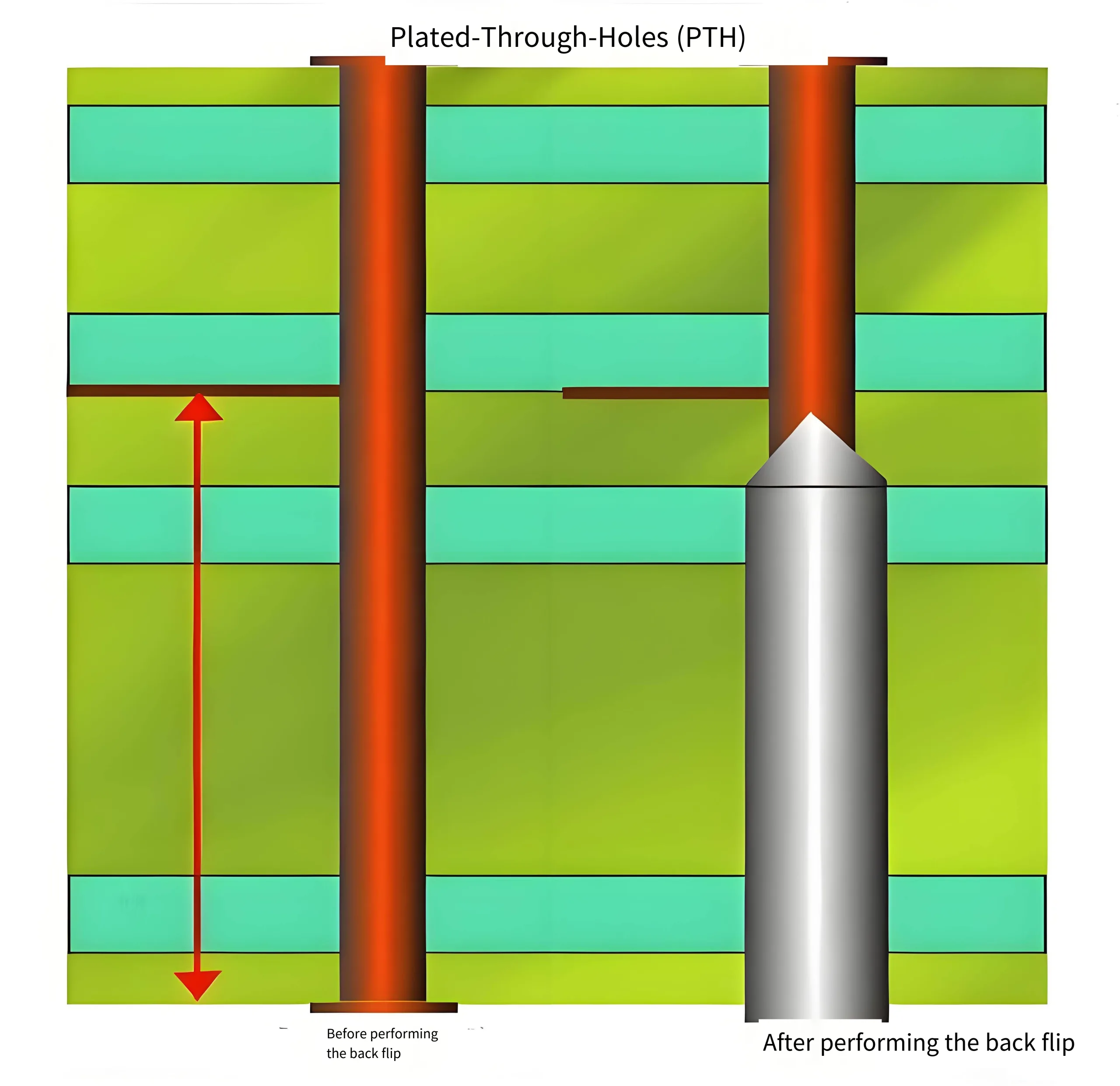
Critical Process: Controlled-Depth Drilling (การขุดเจาะหลัง): In 12-layer or higher PCB หลายชั้น, the unused portion (ต้นขั้ว) of a through-hole via can cause significant signal reflection, degrading integrity. ที่ back drilling process precisely removes this non-functional via stub, eliminating its negative impact—a key technology for high-speed multilayer PCB ผลงาน.
ขั้นตอนการผลิต & การประกันคุณภาพ
UGPCB 12-กระบวนการผลิต PCB ชั้น strictly adheres to มาตรฐาน IPC and includes ออกแบบเพื่อการผลิต (DFM) ทบทวน, inner layer imaging, การเคลือบ, การขุดเจาะ (including back drilling), ชุบ, การถ่ายภาพชั้นนอก, การประยุกต์ใช้หน้ากากประสาน, พื้นผิวเสร็จสิ้น (โอป), การกำหนดเส้นทาง, การทดสอบทางไฟฟ้า, and final inspection. Each stage is supported by precision measurement equipment (Aoi, Impedance Testing, การทดสอบโพรบบิน), ensuring every แผงวงจร delivered meets design specifications and our high-quality standards.
การใช้งานทั่วไป & การจำแนกประเภทผลิตภัณฑ์
This high-performance บอร์ด PCB is designed for demanding electrical environments and complex systems, primarily used in:
-
High-End Network & อุปกรณ์สื่อสาร: มาเธอร์บอร์ดหลักสำหรับโมดูลออปติคอล 400G/800G, เราเตอร์ระดับไฮเอนด์, และสวิตช์.
-
Data Center & คลาวด์คอมพิวติ้ง: เมนบอร์ดเซิร์ฟเวอร์, การ์ดเร่งความเร็ว, storage backplanes.
-
คอมพิวเตอร์ประสิทธิภาพสูง: Workstation motherboards, GPU computing cards, AI accelerator hardware.
-
การทดสอบขั้นสูง & เครื่องมือวัด: Internal boards for instruments processing very high-frequency signals.
การจำแนกประเภทผลิตภัณฑ์ทางวิทยาศาสตร์:
-
โดยการนับเลเยอร์: PCB หลายชั้น (>8 ชั้น)
-
By Technology Type: PCB ความเร็วสูง/ความถี่สูง, เอชดีไอ พีซีบี, PCB ทองแดงหนัก (partial)
-
โดยการสมัคร: Telecom Infrastructure PCB, Data Center/Server PCB
Why Choose UGPCB for Your 12-Layer High-Speed PCB?
-
ความเชี่ยวชาญด้านเทคนิค: Proven mastery of การเจาะกลับ และ ฟอยล์ทองแดง RTF application to tackle high-speed design challenges.
-
การผลิตที่แม่นยำ: Capable of 3/3.5 mil line/space, meeting stringent high-density interconnect requirements.
-
Material Integrity: Core use of reputable high-speed laminates like Nanya NY6300S ensures foundational performance.
-
สนับสนุนการออกแบบ: Expert การออกแบบ PCB และ DFM review services to de-risk your project from the start.
-
Consistent Quality: A fully controlled การผลิต PCB and inspection system delivers reliable products you can trust.
Ready to elevate your hardware? Contact UGPCB’s engineers for a free PCB quote และ การวิเคราะห์ DFM on your next 12-layer high-speed board project.






This internet website might be a walk-through its the data you wanted in regards to this and didnt know who should. Glimpse here, and youll completely discover it.