

1. ภาพรวมผลิตภัณฑ์
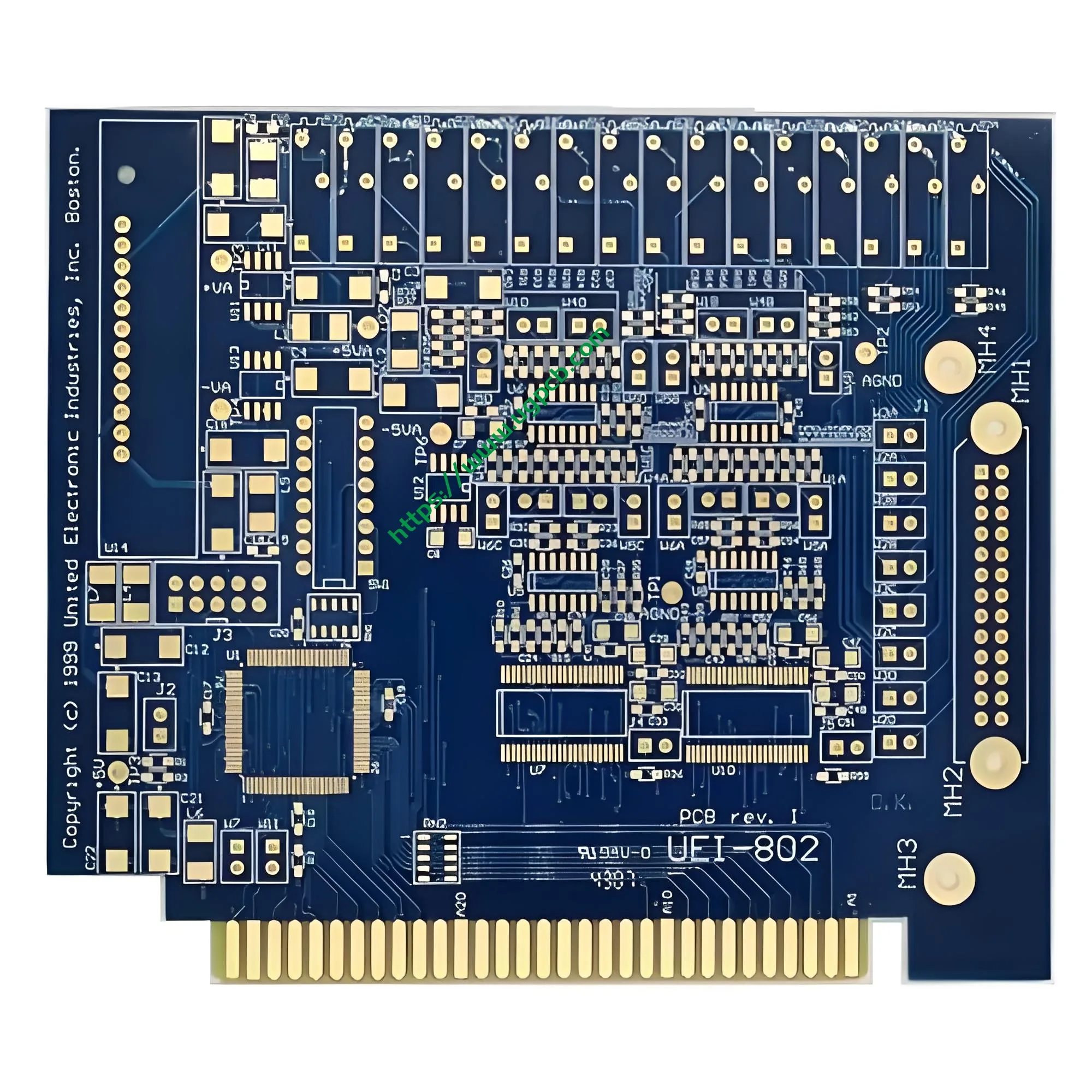
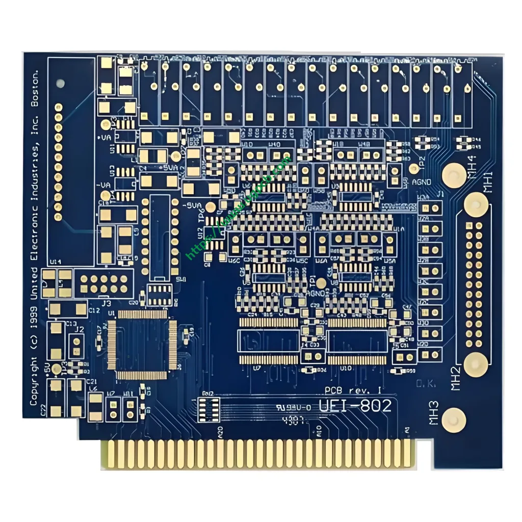
นิ้วทองสองด้าน แผงวงจรพิมพ์ (พีซีบี) มีหน้าสัมผัสเคลือบทอง หรือที่เรียกกันทั่วไปว่า "นิ้วทอง" ซึ่งจัดเรียงตามขอบบอร์ด. หน้าสัมผัสเหล่านี้สร้างเส้นทางไฟฟ้าแบบเสียบได้เมื่อเสียบเข้ากับขั้วต่อผสมพันธุ์, เช่นช่องเสียบการ์ดหรือซ็อกเก็ต. สัญญาณและกำลังทั้งหมดไหลผ่านขั้วต่อรูปนิ้วเหล่านี้.
PCB นิ้วสีทองสองด้านของ UGPCB ใช้ซับสเตรต FR4 ที่มีการออกแบบ 2 ชั้น. ความหนาของบอร์ดคือ 1.6 มม, และทั้งชั้นในและชั้นนอกก็มี 1 ทองแดง. เส้นผ่านศูนย์กลางขั้นต่ำในการเจาะคือ 0.3 มม, และมีทั้งความกว้างและระยะห่างของการติดตาม 0.15 มม. พื้นผิวเป็นสีทองแช่ (เห็นด้วย) ทั่วทั้งกระดาน, พร้อมด้วยทองคำแข็งชุบแข็งแบบไฟฟ้าเพิ่มเติมที่เลือกใช้บริเวณนิ้วทอง. ผลิตภัณฑ์นี้นำเสนอความยืดหยุ่นในการกำหนดเส้นทางของบอร์ดสองด้าน พร้อมด้วยความน่าเชื่อถือที่ได้รับการพิสูจน์แล้วของการเชื่อมต่อแบบนิ้วทอง. รองรับระบบอิเล็กทรอนิกส์ที่หลากหลายที่ต้องใช้อินเทอร์เฟซปลั๊กอินแบบบอร์ดต่อบอร์ด.
2. การจำแนกประเภทและการวางตำแหน่งผลิตภัณฑ์
ตามมาตรฐาน IPC‑6012 (คุณสมบัติและข้อกำหนดด้านประสิทธิภาพของบอร์ดพิมพ์ที่เข้มงวด), ผลิตภัณฑ์นี้จัดอยู่ในประเภทต่อไปนี้:
| มิติการจำแนกประเภท | หมวดหมู่ |
|---|---|
| ตามโครงสร้าง | PCB สองด้าน – มีรอยนำไฟฟ้าทั้งสองด้าน |
| โดยวิธีการเชื่อมต่อโครงข่าย | มีรูชุบทะลุ (พท) |
| ตามคลาสประสิทธิภาพ IPC‑6012 | ระดับ 2 (บริการเฉพาะผลิตภัณฑ์อิเล็กทรอนิกส์) - เหมาะสำหรับงานนิ้วทองส่วนใหญ่ |
| โดยวัสดุพื้นผิว | FR4 ลามิเนตแข็ง (เกรด S1141) |
| โดยพื้นผิวเสร็จสิ้น | เห็นด้วย (นิกเกิลแบบไม่ใช้ไฟฟ้า / ทองคำแช่) + ทองแข็งแบบคัดเลือกด้วยไฟฟ้าบนนิ้วทอง |
| ตามฟังก์ชั่น | PCB นิ้วทอง / PCB ขั้วต่อขอบ |
สินค้าชิ้นนี้อยู่ในตำแหน่งกการเชื่อมต่อปลั๊กอินความน่าเชื่อถือปานกลางถึงสูง สารละลาย. เป็นการผสมผสานการออกแบบอิสระของการกำหนดเส้นทางสองด้านเข้ากับความสมบูรณ์ของสัญญาณของขั้วต่อขอบนิ้วทอง.
3. พารามิเตอร์ทางเทคนิคที่สำคัญ
3.1 พื้นผิว: FR4 + S1141 ลามิเนต
FR4 เป็นสารตั้งต้นที่มีความแข็งมากที่สุดในอุตสาหกรรม PCB. ประกอบด้วยอีพอกซีเรซินเสริมใยแก้ว, ซึ่งให้ความแข็งแรงทางกลที่ดีเยี่ยม, ฉนวนไฟฟ้า, และต้านทานความร้อน. สินค้าชิ้นนี้ใช้ ลามิเนต S1141 FR4 จากเทคโนโลยี Shengyi, ซึ่งสอดคล้องกับ IPC‑4101/21.
ตัวบ่งชี้ประสิทธิภาพหลักสำหรับ S1141 (ทดสอบแล้ว 1.6 ตัวอย่างมม) อยู่ด้านล่าง.
| พารามิเตอร์ | ค่าทั่วไป | วิธีทดสอบ |
|---|---|---|
| อุณหภูมิการเปลี่ยนแก้ว (ทีจี) | 140องศาเซลเซียส (DSC) | IPC‑TM‑650 2.4.25 |
| อุณหภูมิการสลายตัวทางความร้อน (TD) | 310องศาเซลเซียส (5 % การลดน้ำหนัก) | IPC‑TM‑650 2.4.24.6 |
| CTE แกน Z (ก่อนทีจี) | 65 ppm/° C | IPC‑TM‑650 2.4.24 |
| CTE แกน Z (หลังจากทีจี) | 300 ppm/° C | IPC‑TM‑650 2.4.24 |
| ค่าคงที่ไดอิเล็กตริก (ดีเค, 1 เมกะเฮิรตซ์) | 4.6 | IPC‑TM‑650 2.5.5.9 |
| ปัจจัยการกระจาย (ฟ, 1 เมกะเฮิรตซ์) | 0.015 | IPC‑TM‑650 2.5.5.9 |
| คะแนนความไวไฟ | อล 94 วี-0 | อล 94 |
| การดูดซึมน้ำ | 0.15 % | IPC‑TM‑650 2.6.2.1 |
แหล่งข้อมูล: เอกสารข้อมูลทางเทคนิค Shengyi S1141, สอดคล้องกับ IPC‑4101/21.
อล 94 วี-0 เป็นระดับการหน่วงไฟสูงสุดใน UL 94 การทดสอบการเผาไหม้ในแนวตั้ง. กำหนดให้หลังจากการใช้เปลวไฟ 10 วินาทีสองครั้ง, เวลาการเผาไหม้รวมของแต่ละชิ้นงานจะต้องไม่เกิน 10 ไม่กี่วินาที, และไม่มีเปลวไฟหยดติดไฟตัวบ่งชี้ฝ้าย. ซึ่งช่วยให้มั่นใจได้ว่า PCB ยังคงปลอดภัยภายใต้สภาวะความร้อนที่ผิดปกติหรือการลัดวงจร.

3.2 ความหนาของบอร์ด: 1.6 มม
ที่ 1.6 ความหนา มม. เป็นมาตรฐานอุตสาหกรรมสำหรับ PCB แบบแข็ง. นอกจากนี้ยังทำหน้าที่เป็นความหนาพื้นฐานสำหรับข้อมูลคุณสมบัติของวัสดุ S1141. ความหนานี้ทำให้เกิดความสมดุลที่เหมาะสมระหว่างความแข็งแรงเชิงกล, ความมั่นคงในการแทรก, และต้นทุนการผลิต. สามารถใช้งานร่วมกับช่องเชื่อมต่อมาตรฐานได้อย่างกว้างขวาง.
3.3 ความหนาของทองแดง: 1 ออนซ์ (ประมาณ 35 μm)
มีทั้งแผ่นฟอยล์ทองแดงชั้นในและชั้นนอก1 ออนซ์ (ออนซ์) , ซึ่งก็ประมาณนั้น 35 หนา ไมครอน. ตามมาตรฐาน IPC‑6012, ความหนาทองแดงสำเร็จรูปขั้นต่ำสำหรับคลาส 1 และชั้นเรียน 2 บอร์ดคือ 48 μm. เริ่มด้วย 1 ฟอยล์ออนซ์ช่วยให้มั่นใจได้ว่าความหนาสุดท้ายหลังการประมวลผลตรงตามข้อกำหนดเหล่านี้. ตุ้มน้ำหนักทองแดงนี้รองรับความสามารถในการจ่ายกระแสไฟที่เพียงพอ (ประมาณ 4-6 A, ขึ้นอยู่กับความกว้างของรอย) ในขณะที่ยังคงรักษาความแม่นยำในการแกะสลักแบบละเอียด. ความกว้างของการติดตามและระยะห่างของ 0.15 มม (เกี่ยวกับ 6 MIL) สามารถผลิตได้อย่างน่าเชื่อถือด้วย 1 ทองแดง.
3.4 เส้นผ่านศูนย์กลางขั้นต่ำ: 0.3 มม
เส้นผ่านศูนย์กลางรูเจาะเชิงกลขั้นต่ำคือ 0.3 มม, ซึ่งอยู่ในความสามารถด้านเทคโนโลยีรูทะลุมาตรฐาน. รองรับการชุบรูทะลุ (พท) การประมวลผลเพื่อให้แน่ใจว่าการเชื่อมต่อทางไฟฟ้าที่เชื่อถือได้ระหว่างชั้น. สำหรับ IPC-6012, PTH ทั้งหมดจะต้องผ่านการทดสอบความเครียดจากความร้อน (288 บัดกรีจุ่ม° C) เพื่อตรวจสอบความสมบูรณ์ของโครงสร้าง.
3.5 ติดตามความกว้างและระยะห่าง: 0.15 มม / 0.15 มม
ความกว้างการติดตามของ 0.15 มม (ประมาณ 6 MIL) และระยะห่างของ 0.15 มม. แสดงถึงความสามารถแบบละเอียดในการผลิต PCB ทั่วไป. ที่ 1 ความหนาทองแดง, อัน 0.15 มม. สามารถส่งกระแสได้ประมาณ 0.5-0.8 A ตามการคำนวณ IPC-2221. ซึ่งตอบสนองความต้องการของการใช้งานการส่งสัญญาณและแหล่งจ่ายไฟต่ำส่วนใหญ่. การผสมผสานระหว่างความกว้างและระยะห่างนี้ทำให้มั่นใจได้ถึงความน่าเชื่อถือในขณะเดียวกันก็รักษาต้นทุนการผลิตให้อยู่ภายใต้การควบคุม.
4. พื้นผิวเสร็จสิ้น: Immersion Gold บวกกับนิ้วทองชุบด้วยไฟฟ้า
ผลิตภัณฑ์นี้ใช้กกระบวนการตกแต่งพื้นผิวแบบผสมผสาน: ทองคำแช่ (เห็นด้วย) ทั่วทั้งกระดาน, กับทองคำแข็งชุบด้วยไฟฟ้า เลือกใช้เฉพาะบริเวณนิ้วทอง. นี่เป็นกระบวนการมาตรฐานและเหมาะสมที่สุดสำหรับ PCB แบบนิ้วทอง.
4.1 ทองแช่ (เห็นด้วย) กระบวนการ
นิกเกิลแบบไม่ใช้ไฟฟ้า / ทองแช่ (เห็นด้วย) เป็นการเคลือบผิวที่นิกเกิลถูกวางทางเคมีลงบนพื้นผิวทองแดงเป็นครั้งแรก, ตามด้วยชั้นทองคำบางๆ ที่สะสมตัวผ่านปฏิกิริยาการแทนที่.
ต่อIPC‑4552 การแก้ไข A (ออกแล้ว 2017) :
- ความหนาของนิกเกิล: 3 ไมโครเมตรถึง 6 μm (120 μinถึง 240 นาที)
- ทองหนา: 0.04 ไมโครเมตรถึง 0.10 μm (1.6 μinถึง 4.0 นาที)
- ความหนาของทองคำที่แนะนำ: 0.04 ไมโครเมตรถึง 0.07 μm (1.6 μinถึง 2.8 นาที)
แหล่งข้อมูล: IPC‑4552 – ข้อมูลจำเพาะด้านประสิทธิภาพสำหรับนิกเกิลแบบไม่ใช้ไฟฟ้า / ทองแช่ (เห็นด้วย) การชุบสำหรับบอร์ดพิมพ์.
ข้อดีของ ENIG:
- พื้นผิวเรียบเหมาะสำหรับการติดตามระยะพิทช์ละเอียดและแพ็คเกจ BGA
- ความสามารถในการบัดกรีดีเยี่ยม รองรับการบัดกรีไร้สารตะกั่ว (เช่น, SAC305)
- ต้านทานการเกิดออกซิเดชันที่รุนแรงพร้อมอายุการเก็บรักษาที่ยาวนาน
- ชั้นทองบางช่วยให้บริหารจัดการต้นทุนได้
4.2 นิ้วทองชุบไฟฟ้า – คุณสมบัติหลัก
บริเวณนิ้วทองได้รับทองคำแข็งชุบด้วยไฟฟ้าเพิ่มเติม. ต่างจากทองคำอ่อนที่ใช้ใน ENIG, ทองคำแข็งชุบด้วยไฟฟ้า มีสารทำให้แข็งเช่นโคบอลต์หรือนิกเกิล (โลหะผสมทอง-โคบอลต์หรือทอง-นิกเกิล). ความแข็งสามารถเกิน HV 200, ให้ความทนทานต่อการสึกหรอมากกว่าทองคำอ่อนมาก.
เหตุใดนิ้วทองจึงต้องใช้ทองคำแข็งที่ชุบด้วยไฟฟ้า?
ทองคำ ENIG มีความบางมาก (เพียง 0.04-0.10 ไมโครเมตร) และอ่อนนุ่ม (ความแข็งต่ำกว่า HV 90). มันจะสึกหรอหลังจากใส่เพียง 3-5 รอบ. ชุบทองแข็งด้วยไฟฟ้า, ที่มีความหนามากกว่าปกติ 0.76 μm, สามารถทนต่อการแทรกได้หลายร้อยหรือหลายพันรอบ.
ต่อไอพีซี-4556 (ข้อมูลจำเพาะด้านประสิทธิภาพฮาร์ดโกลด์) :
| คลาสแอปพลิเคชัน | ความหนาทองขั้นต่ำ | การใช้งานทั่วไป |
|---|---|---|
| ระดับ 2 (ทนทาน) | ≥ 0.76 μm (30 นาที) | แอพพลิเคชั่นนิ้วทองส่วนใหญ่ |
| ระดับ 3 (ความน่าเชื่อถือสูง) | ≥ 1.27 μm (50 นาที) | การแทรกรอบสูง, ทางอุตสาหกรรม / ทหาร |
| นิกเกิลอันเดอร์เลเยอร์ | 3−5 ไมโครเมตร | จำเป็นสำหรับการฝากทองคำแข็งทั้งหมด |
แหล่งข้อมูล: IPC‑4556 – ข้อมูลจำเพาะด้านประสิทธิภาพสำหรับทองคำแข็งชุบไฟฟ้าสำหรับตัวเชื่อมต่อและนิ้วทอง.
กระบวนการชุบทองด้วยไฟฟ้าที่ใช้ในผลิตภัณฑ์นี้เป็นไปตามคลาส IPC‑4556 2 ผ่านชั้นเรียน 3 มาตรฐาน, ทำให้มั่นใจได้ถึงอายุการใช้งานและความน่าเชื่อถือของหน้าสัมผัส.
5. ข้อควรพิจารณาในการออกแบบ
5.1 การลบมุมนิ้วทอง
ปลายนิ้วทองสอดต้องอยู่ลบมุม เพื่อให้สามารถเข้าสู่ช่องเชื่อมต่อได้อย่างราบรื่น.
- มุมลบมุม: โดยทั่วไป 30° หรือ 45°
- ความลึกของการลบมุม: สำหรับ 1.6 ความหนาของบอร์ด มม, โดยทั่วไปความลึกของการลบมุมจะอยู่ที่ 0.8-1.0 มม, เหลือขอบทื่อ 0.6-0.8 มม. ที่ส่วนปลาย
- ความหนาของปลายที่เหลืออยู่: ประมาณหนึ่งในสามถึงครึ่งหนึ่งของความหนาของกระดานเดิม
- ข้อกำหนดที่สำคัญ: ไม่มีหน้ากากประสานอาจครอบคลุมพื้นที่ลบมุม, และชั้นทองจะต้องครอบคลุมมุมเอียงที่ลบมุมจนหมด
5.2 กฎการออกแบบพื้นที่นิ้วทอง
- ควรวางนิ้วทองไว้ที่ขอบกระดานตามลำดับ
- ระยะห่างขั้นต่ำระหว่างนิ้วทองที่อยู่ติดกันควรเป็น ≥ 7 MIL (ประมาณ 0.178 มม)
- บริเวณนิ้วทองจะต้องทำเครื่องหมายไว้อย่างชัดเจนในไฟล์ Gerber พร้อมคำแนะนำในการชุบอย่างชัดเจน
5.3 ข้อควรพิจารณาในการควบคุมความต้านทาน
วัสดุ FR4 มีค่าคงที่ไดอิเล็กทริก Dk = 4.6 ที่ 1 เมกะเฮิรตซ์. สำหรับ 50 Ω ปลายเดี่ยวหรือ 100 Ω การควบคุมอิมพีแดนซ์แบบดิฟเฟอเรนเชียล, นักออกแบบสามารถปรับความกว้างของรอยเส้นและความหนาของอิเล็กทริกได้. ที่ 0.15 ความกว้างและระยะห่างของรอยเส้น มม. ในผลิตภัณฑ์นี้ตรงตามข้อกำหนดความสมบูรณ์ของสัญญาณส่วนใหญ่สำหรับการออกแบบมาตรฐาน.
6. หลักการทำงาน
PCB นิ้วสีทองสองด้านทำงานผ่านกลไกหลักสองประการ: หน้าสัมผัสทางไฟฟ้า และการส่งสัญญาณ.
- การเชื่อมต่อไฟฟ้า: หน้าสัมผัสนิ้วทองที่ขอบบอร์ดจะจับคู่กับหน้าสัมผัสสปริงโลหะภายในช่องตัวเชื่อมต่อ, สร้างเส้นทางไฟฟ้าความต้านทานต่ำ.
- การส่งสัญญาณ: PCB ติดตามสัญญาณเส้นทางจากต่างๆ ส่วนประกอบ (ชิป, ตัวต้านทาน, ตัวเก็บประจุ, ฯลฯ) ไปที่หน้าสัมผัสนิ้วทอง, ซึ่งจะส่งผ่านขั้วต่อไปยังเมนบอร์ดหรือแบ็คเพลน. การออกแบบสองด้านช่วยให้สามารถกำหนดเส้นทางได้ ทั้งชั้นบนและชั้นล่าง, เพิ่มความหนาแน่นของเส้นทางและความยืดหยุ่นในการออกแบบอย่างมาก.
- ความสามารถในการเสียบปลั๊ก: ชั้นทองคำแข็งที่ชุบด้วยไฟฟ้าบนนิ้วทองมีความทนทานต่อการสึกหรอเพียงพอเพื่อรองรับรอบการแทรกหลายรอบ โดยไม่ลดความต้านทานการสัมผัสหรือความสมบูรณ์ของสัญญาณ.
7. แอปพลิเคชันและกรณีการใช้งาน
PCB นิ้วทองสองด้านถูกนำมาใช้กันอย่างแพร่หลายในอุปกรณ์อิเล็กทรอนิกส์ที่ต้องการการเชื่อมต่อแบบเสียบได้. แอปพลิเคชันทั่วไปรวมถึง:
| พื้นที่ใช้งาน | ผลิตภัณฑ์เฉพาะ |
|---|---|
| การคำนวณ & เซิร์ฟเวอร์ | โมดูลหน่วยความจำ (ดีดีอาร์, DDR2, DDR3, DDR4, DDR5), กราฟิกการ์ด, การ์ดเชื่อมต่อเครือข่าย, การ์ดขยาย |
| อุปกรณ์อิเล็กทรอนิกส์สำหรับผู้บริโภค | ไดรฟ์ USB, การ์ดหน่วยความจำ, เครื่องอ่านการ์ด, สมาร์ทโฟน, สมาร์ทวอทช์ |
| อุปกรณ์สื่อสาร | เราเตอร์, สวิตช์, โมดูลการสื่อสาร |
| การควบคุมอุตสาหกรรม | แผงควบคุมอุตสาหกรรม, การ์ดเก็บข้อมูล, ติดตั้งการทดสอบ |
| อุปกรณ์อิเล็กทรอนิกส์ยานยนต์ | ชุดควบคุมภายในรถยนต์, ระบบสาระบันเทิง |
| อุปกรณ์การแพทย์ | โมดูลอิเล็กทรอนิกส์ทางการแพทย์ (พร้อมอาหารเสริมทางการแพทย์ IPC‑6012EM) |
| การบินและอวกาศ | โมดูล Avionics (พร้อมอุปกรณ์เสริมด้านการบินและอวกาศ IPC‑6012FS) |
PCB นิ้วทองสองด้าน FR4 เหมาะอย่างยิ่งสำหรับความซับซ้อนปานกลาง, การใช้งานที่คำนึงถึงต้นทุน ที่ต้องการการเชื่อมต่อปลั๊กอิน.
8. ผังกระบวนการผลิต
UGPCB ปฏิบัติตามลำดับการผลิตมาตรฐานสำหรับ PCB สีทองสองด้าน:
- การตัด – ตัดลามิเนตหุ้มทองแดง FR4 ให้ได้ขนาดแผงการทำงาน.
- การขุดเจาะ - เจาะ 0.3 รูทะลุ มม. และรูยึด.
- พท / การชุบแผง – ใช้การสะสมทองแดงโดยไม่ใช้ไฟฟ้าในรู, แล้วแผ่นแผง.
- การถ่ายโอนรูปแบบ – เปิดเผยและพัฒนารูปแบบวงจร.
- การชุบลวดลาย – ชุบวงจรและรูด้วยไฟฟ้า 1 ทองแดง.
- การแกะสลัก – ลอกฟอยล์ทองแดงที่ไม่มีการป้องกันออกเพื่อสร้างรอยวงจรขั้นสุดท้าย.
- หน้ากากบัดกรี – ใช้หมึกหน้ากากประสานสีเขียวหรือสีอื่น ๆ.
- การตกแต่งพื้นผิว – ENIG – ทานิกเกิลแบบไม่ใช้ไฟฟ้าและทองแช่ให้ทั่วทั้งกระดาน.
- การชุบนิ้วทองคำ – ชุบทองแข็งด้วยไฟฟ้าแบบคัดเลือกบริเวณนิ้วทอง.
- การลบมุมนิ้วทอง – ลบคมส่วนท้ายของการแทรก.
- การทดสอบทางไฟฟ้า - ดำเนินการ โพรบบิน หรือการทดสอบฟิกซ์เจอร์.
- การตรวจสอบภาพ – ตรวจสอบตาม IPC‑A‑600.
- การบรรจุ & การส่งสินค้า – แพ็คสูญญากาศเพื่อป้องกันความชื้น.
9. ประสิทธิภาพและมาตรฐานคุณภาพ
ผลิตภัณฑ์นี้ได้รับการออกแบบและผลิตตามมาตรฐานสากลต่อไปนี้อย่างเคร่งครัด:
| มาตรฐาน | ชื่อ | ขอบเขต |
|---|---|---|
| ไอพีซี-6012 | ข้อกำหนดคุณสมบัติและประสิทธิภาพสำหรับบอร์ดพิมพ์แข็ง | ประสิทธิภาพโดยรวมและความน่าเชื่อถือ |
| IPC-A-600 | การยอมรับของบอร์ดพิมพ์ | รูปลักษณ์ภายนอกและเกณฑ์การยอมรับ |
| ไอพีซี-4552 | ข้อมูลจำเพาะด้านประสิทธิภาพของ ENIG | การควบคุมกระบวนการแช่ทอง |
| ไอพีซี-4556 | ข้อมูลจำเพาะด้านประสิทธิภาพทองคำแข็งชุบไฟฟ้า | นิ้วทองกระบวนการทองแข็ง |
| IPC-4101/21 | ข้อกำหนดสำหรับวัสดุพื้นผิวบอร์ดพิมพ์แข็งและหลายชั้น | ข้อมูลจำเพาะของวัสดุ FR4 |
| อล 94 วี-0 | มาตรฐานความปลอดภัย – ความไวไฟของวัสดุพลาสติก | การรับรองสารหน่วงไฟ |
10. ทำไมต้องเลือก UGPCB?
- ประสบการณ์การผลิตนิ้วทองระดับมืออาชีพ – UGPCB มีขีดความสามารถที่ครบถ้วนในการชุบด้วยไฟฟ้าและการลบมุม.
- การควบคุมคุณภาพตั้งแต่ต้นจนจบ – ทุกขั้นตอนตั้งแต่การตัดจนถึงการตรวจสอบขั้นสุดท้ายได้รับการจัดการตามมาตรฐาน IPC.
- วัสดุที่ตรวจสอบย้อนกลับได้ – ใช้ลามิเนต FR4 แบรนด์เนม เช่น Shengyi S1141 พร้อมการตรวจสอบแหล่งที่มาที่ชัดเจน.
- จัดส่งที่รวดเร็ว – สายการผลิต PCB สองด้านโดยเฉพาะรองรับการสร้างต้นแบบอย่างรวดเร็วและการผลิตในปริมาณมาก.
- การสนับสนุนด้านเทคนิค – ให้ DFM (ออกแบบเพื่อการผลิต) บทวิจารณ์และคำแนะนำในการควบคุมอิมพีแดนซ์.
11. สอบถามตอนนี้
UGPCB มุ่งมั่นที่จะนำเสนอโซลูชัน PCB นิ้วทองสองด้านที่มีมูลค่าสูงให้แก่ลูกค้าทั่วโลก. ไม่ว่าคุณจะต้องการการสร้างต้นแบบตัวอย่าง, การทดลองผลิตชุดเล็ก, หรือการผลิตในปริมาณมาก, เรามีความเชี่ยวชาญที่จะให้บริการคุณ.
ติดต่อเราเพื่อขอใบเสนอราคา:
- จัดเตรียมไฟล์ Gerber หรือ การออกแบบ PCB ข้อมูล
- ระบุความหนาของการชุบนิ้วทอง (0.76 ไมโครเมตรถึง 1.27 ไมโครเมตรแนะนำ)
- ยืนยันมุมลบมุม (30°หรือ 45°) และข้อกำหนดพิเศษอื่น ๆ
การประกาศแหล่งข้อมูล
ข้อมูลทางเทคนิคและข้อมูลอ้างอิงมาตรฐานในเอกสารนี้มีที่มาจาก: ข้อมูลจำเพาะด้านคุณสมบัติและประสิทธิภาพของ IPC‑6012 สำหรับบอร์ดพิมพ์แบบแข็ง; ข้อมูลจำเพาะด้านประสิทธิภาพ IPC‑4552 สำหรับนิกเกิลแบบไม่ใช้ไฟฟ้า / ทองแช่ (เห็นด้วย) การชุบสำหรับบอร์ดพิมพ์; ข้อมูลจำเพาะด้านประสิทธิภาพ IPC‑4556 สำหรับฮาร์ดโกลด์ชุบไฟฟ้าสำหรับตัวเชื่อมต่อและนิ้วทอง; การยอมรับ IPC‑A‑600 ของบอร์ดแบบพิมพ์; อล 94 มาตรฐานความปลอดภัย – ความไวไฟของวัสดุพลาสติก; และเอกสารข้อมูลทางเทคนิค Shengyi S1141 (สอดคล้องกับ IPC‑4101/21).













