


ฉัน. ภาพรวมผลิตภัณฑ์
บอร์ด PCB แบบทะลุรูสองด้าน UGPCB เป็นบอร์ดชนิดแข็ง 2 ชั้นประสิทธิภาพสูง แผงวงจรพิมพ์ สร้างบนพื้นผิวอีพ็อกซี่แก้ว FR-4 โดยใช้รูทะลุชุบ (พท) เทคโนโลยี. คณะกรรมการมีมาตรการ 86.9 × 73.58 มม. มีความหนา 1.0 มม, ความหนาของฟอยล์ทองแดงของ 1/1 ออนซ์ (35 µm ทั้งชั้นนอกและชั้นใน), และการปรับระดับการบัดกรีด้วยลมร้อนไร้สารตะกั่ว (เลือดออก) พื้นผิวเสร็จสิ้น. หน้ากากประสานเป็นสีเขียว, และตำนานซิลค์สกรีนเป็นสีขาว.
PCB รูทะลุสองด้าน (แผงวงจรพิมพ์สองด้าน) มีวงจรนำไฟฟ้าทั้งสองด้านของพื้นผิวฉนวน, มีรูทะลุชุบให้สามารถเชื่อมต่อไฟฟ้าระหว่างสองชั้นได้. เปรียบเทียบกับ PCB ด้านเดียว, PCB สองด้านมีความหนาแน่นในการกำหนดเส้นทางที่สูงขึ้น 60%–80% และรองรับการออกแบบวงจรที่ซับซ้อนมากขึ้น. UGPCB, ได้รับการสนับสนุนจากระบบคุณภาพที่ได้รับการรับรองมาตรฐาน ISO และกระบวนการผลิตที่สอดคล้องกับ IPC, มอบ PCBs รูทะลุสองด้านคุณภาพสูงและแบบครบวงจร พีซีบี บริการแก่ผู้ผลิตอุปกรณ์อิเล็กทรอนิกส์ทั่วโลก.
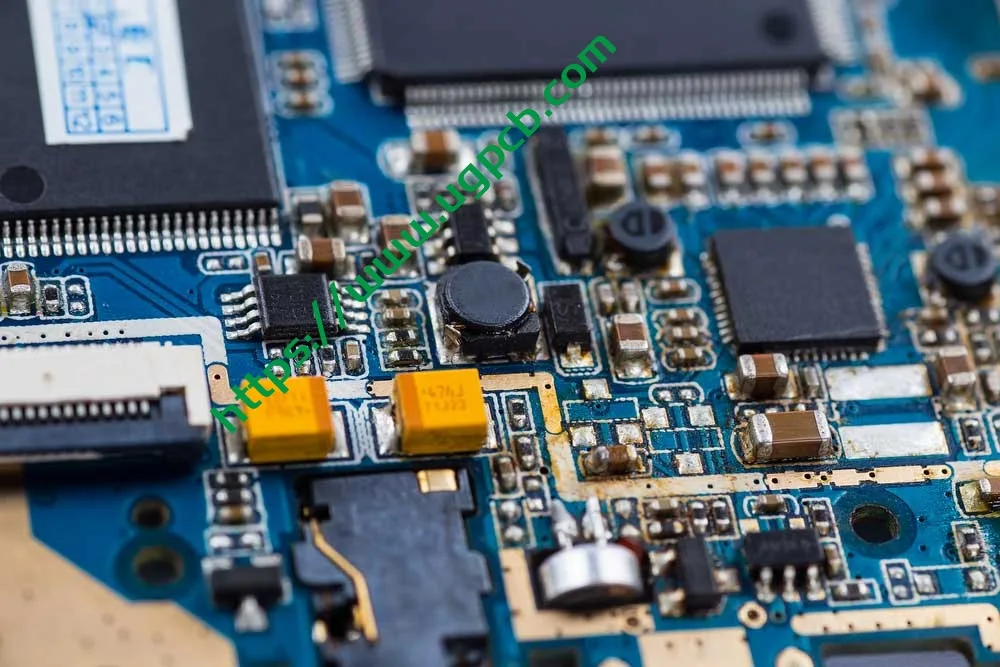
ครั้งที่สอง. คำจำกัดความของผลิตภัณฑ์และข้อกำหนดทางเทคนิค
ต่อ IPC-6012F ข้อกำหนดคุณสมบัติและประสิทธิภาพสำหรับบอร์ดพิมพ์แข็ง (เผยแพร่เมื่อเดือนกันยายน 2023), PCB รูทะลุสองด้านจัดเป็นบอร์ดพิมพ์แข็งพร้อมรูทะลุชุบ (พิมพ์ 2). คุณลักษณะหลักของมันคือการเชื่อมต่อทางไฟฟ้าระหว่างตัวนำทั้งสองด้านผ่านผนังรูที่ชุบทองแดง. UGPCB ผลิตผลิตภัณฑ์นี้ตามมาตรฐาน IPC-6012F อย่างสมบูรณ์และตรงตาม Class 2 ข้อกำหนดด้านประสิทธิภาพ (อุปกรณ์อิเล็กทรอนิกส์บริการเฉพาะ).
ข้อกำหนดที่สำคัญ:
| พารามิเตอร์ | ข้อมูลจำเพาะ |
|---|---|
| วัสดุพื้นผิว | FR-4 (สารหน่วงไฟ UL 94 วี-0) |
| จำนวนเลเยอร์ | 2 ชั้น (สองด้าน) |
| ความหนาของบอร์ด | 1.0 มม |
| ขนาดบอร์ด | 86.9 × 73.58 มม |
| เส้นผ่านศูนย์กลางรูขั้นต่ำ | 0.236 มม |
| ความกว้างบรรทัดขั้นต่ำ / ระยะห่าง | 0.32 × 0.37 มม |
| ความหนาของฟอยล์ทองแดง | 1/1 ออนซ์ (ประมาณ. 35 ไมโครเมตรในแต่ละด้าน) |
| พื้นผิวเสร็จสิ้น | HASL ไร้สารตะกั่ว (การปรับระดับการบัดกรีด้วยอากาศร้อน) |
| หน้ากากบัดกรี / ตำนาน | หน้ากากประสานสีเขียว / ซิลค์สกรีนสีขาว |
ที่สาม. แนวทางการออกแบบ
3.1 การเลือกวัสดุพื้นผิว — มูลค่าทางวิศวกรรมของ FR-4
FR-4 เป็นการกำหนดเกรดสารหน่วงไฟที่ก่อตั้งโดยสมาคมผู้ผลิตไฟฟ้าแห่งชาติ (ไม่มี). ตัวอักษร “ศ” ย่อมาจากสารหน่วงไฟ, และหมายเลข “4” หมายถึงระบบอีพอกซีเรซินที่เสริมด้วยผ้าใยแก้วทอ. สำหรับ IPC-4101 ข้อกำหนดสำหรับวัสดุฐานสำหรับบอร์ดพิมพ์แข็งและหลายชั้น, FR-4 เกรด A1 แสดงถึงระดับประสิทธิภาพหลักที่มีความแข็งแรงเชิงกลที่เหมาะสมที่สุด, คุณสมบัติทางไฟฟ้า, และความน่าเชื่อถือในระยะยาว.
ตัวชี้วัดประสิทธิภาพที่สำคัญของ FR-4 (แหล่งที่มา: IPC-4101 และมาตรฐานอุตสาหกรรม):
-
อุณหภูมิการเปลี่ยนแก้ว (ทีจี): 130–140°ซ (มาตรฐาน FR-4)
-
ค่าคงที่ไดอิเล็กตริก (ดีเค) @ 1 กิกะเฮิรตซ์: 4.2–4.5
-
ปัจจัยการกระจาย (ฟ) @ 1 กิกะเฮิรตซ์: ≤ 0.020
-
คะแนนความไวไฟ: อล 94 วี-0
-
การดูดซึมน้ำ (24 ชั่วโมง): ≤ 0.10%
FR-4 ยังคงเป็นวัสดุซับสเตรตที่โดดเด่นในอุตสาหกรรม PCB เนื่องจากมีความสมดุลที่โดดเด่นในด้านความแข็งแรงเชิงกล, ฉนวนไฟฟ้า, เสถียรภาพมิติ, และความสามารถในการแปรรูป.
3.2 มาตรฐานการออกแบบวงจรตาม IPC-2221
สำหรับ IPC-2221 มาตรฐานทั่วไปเกี่ยวกับการออกแบบแผ่นพิมพ์, การออกแบบความกว้างของตัวนำต้องคำนึงถึงความสามารถในการรับกระแสไฟฟ้าด้วย, อุณหภูมิที่เพิ่มขึ้น, และความหนาของทองแดง. สูตรกำลังการผลิตปัจจุบันของ IPC-2221 คือ:
ผม = k · ΔT^0.44 · A^0.725
ที่ไหน:
-
I = ความสามารถในการรองรับกระแสไฟฟ้าสูงสุด (อัน)
-
k = ค่าคงที่เชิงประจักษ์ (0.048 สำหรับชั้นภายนอก, 0.024 สำหรับชั้นภายใน)
-
ΔT = อุณหภูมิที่เพิ่มขึ้นที่อนุญาต (องศาเซลเซียส)
-
A = พื้นที่หน้าตัดของตัวนำ (ล้าน²), โดยที่ A = W × T
ผลิตภัณฑ์ของ UGPCB มีความกว้างของเส้น 0.32 มม (ประมาณ. 12.6 MIL), ระยะห่างบรรทัดของ 0.37 มม (ประมาณ. 14.6 MIL), และความหนาของทองแดง 1 ออนซ์ (35 μm). สำหรับการติดตามชั้นภายนอกที่มีอุณหภูมิเพิ่มขึ้น 10°C:
เอ = 0.32 มม. × 0.035 มม. = 0.0112 มม.² data 17.36 ล้าน²
ฉัน = 0.048 × 10^0.44 × 17.36^0.725 data 0.048 × 2.75 × 7.82 data 1.03 อัน
ความกว้างของตัวนำนี้รองรับโดยประมาณ 1 ก. ของกระแส, ตอบสนองความต้องการด้านพลังงานและการส่งสัญญาณของอุปกรณ์อิเล็กทรอนิกส์สำหรับผู้บริโภคและอุปกรณ์ควบคุมทางอุตสาหกรรมส่วนใหญ่. IPC-2221 แนะนำให้จำกัดอุณหภูมิที่เพิ่มขึ้นสูงสุดไว้ที่ 10°C หรือ 20°C เพื่อรักษาอายุการใช้งาน PCB.
3.3 การออกแบบเส้นผ่านศูนย์กลางรูและอัตราส่วนภาพ
อัตราส่วนภาพของรูทะลุเป็นตัวชี้วัดที่สำคัญสำหรับการประเมินความยากของการเจาะและความยากในการชุบโลหะของรู. สูตรก็คือ:
อัตราส่วนภาพ = ความหนาของบอร์ด / เส้นผ่านศูนย์กลางรูเจาะ
สำหรับผลิตภัณฑ์ของ UGPCB ด้วย 1.0 ความหนาของบอร์ด มม. และ 0.236 มม. เส้นผ่านศูนย์กลางรูขั้นต่ำ:
อัตราส่วนภาพ = 1.0 / 0.236 data 4.24:1
อัตราส่วนภาพนี้ต่ำกว่าขีดจำกัดบนที่อุตสาหกรรมแนะนำอย่างมาก 10:1 และเกณฑ์การออกแบบแบบอนุรักษ์นิยมของ 8:1. บ่งชี้ถึงความยากต่ำในการเจาะและการทำให้เป็นโลหะ, อัตราผลตอบแทนสูง, ต้นทุนที่ควบคุมได้, และมั่นใจในความน่าเชื่อถือตลอดรู.
3.4 อ้างอิงการออกแบบรูปแบบที่ดิน
สำหรับ IPC-7351 ข้อกำหนดทั่วไปสำหรับการออกแบบการติดตั้งบนพื้นผิวและมาตรฐานรูปแบบพื้นดิน, การออกแบบรูปแบบพื้นดินต้องให้แน่ใจว่ามีการสร้างเนื้อประสานที่เพียงพอและมีคุณสมบัติในการบัดกรี, การตรวจสอบได้, และข้อกำหนดความสามารถในการทำงานซ้ำได้. สำหรับส่วนประกอบของรูทะลุ, โดยทั่วไปแนะนำให้ใช้เส้นผ่านศูนย์กลางของดินที่ 1.8–2.2 เท่าของเส้นผ่านศูนย์กลางรูเพื่อให้แน่ใจว่ามีความกว้างของวงแหวนวงแหวนเพียงพอ.
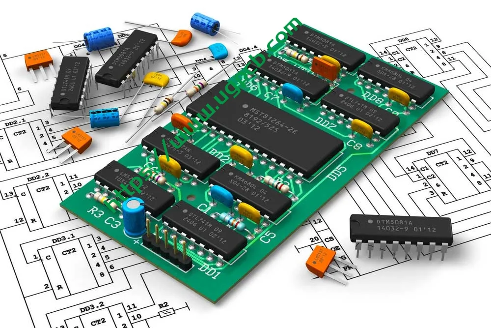
IV. หลักการทำงาน
PCB ทะลุผ่านสองด้านทำงานโดยใช้เทคโนโลยีหลักสามประการ:
1. การกำหนดเส้นทางสองด้าน — รูปแบบวงจรสื่อกระแสไฟฟ้าถูกสลักไว้บนพื้นผิวทั้งด้านบนและด้านล่างของซับสเตรตฉนวน FR-4, ช่วยให้สามารถวางส่วนประกอบได้ทั้งสองด้าน. สิ่งนี้จะเพิ่มความหนาแน่นของวงจรและความยืดหยุ่นในการออกแบบอย่างมาก.
2. ชุบทะลุรู (พท) การเชื่อมต่อโครงข่าย — หลังจากเจาะ, การสะสมของทองแดงโดยไม่ใช้ไฟฟ้าและการชุบทองแดงด้วยไฟฟ้าจะสร้างชั้นสื่อกระแสไฟฟ้าบนผนังรู. สิ่งนี้จะสร้างความต้านทานต่ำ, การเชื่อมต่อทางไฟฟ้าที่เชื่อถือได้สูงระหว่างชั้นบนและชั้นล่าง. ต่อคลาส IPC-6012F 2, ความหนาของทองแดงชุบเฉลี่ยขั้นต่ำบนผนังรูจะต้องเท่ากับ ≥ 20 μm.
3. การประกอบชิ้นส่วนและการบัดกรี — ส่วนประกอบถูกติดตั้งผ่านรู (tht) หรือติดบนพื้นผิว (SMT) เทคนิคและการเชื่อมต่อทางไฟฟ้าผ่านการบัดกรีแบบรีโฟลว์หรือการบัดกรีแบบคลื่น, ผลิต PCBA ที่ทำงานได้อย่างสมบูรณ์ (ชุดประกอบแผงวงจรพิมพ์) โมดูล.
วี. การจำแนกประเภทผลิตภัณฑ์
ตามระบบการจำแนกประเภท IPC-6012F สำหรับบอร์ดพิมพ์แบบแข็ง, สินค้าของ UGPCB จำแนกได้ดังนี้:
| มิติการจำแนกประเภท | หมวดหมู่ |
|---|---|
| โดยการก่อสร้าง | บอร์ดพิมพ์แข็งพร้อมรูทะลุชุบ, สองด้าน (ประเภท IPC-6012F 2) |
| ตามระดับประสิทธิภาพ | ระดับ 2 (บริการเฉพาะด้านอุปกรณ์อิเล็กทรอนิกส์) |
| โดยวัสดุพื้นผิว | FR-4 ลามิเนตผ้าแก้วอีพ็อกซี่ (IPC-4101/21) |
| โดยการนับเลเยอร์ | 2-คณะกรรมการชั้น |
| โดยพื้นผิวเสร็จสิ้น | HASL ไร้สารตะกั่ว |
| ตามระดับความไวไฟ | อล 94 วี-0 |
ตามโดเมนแอปพลิเคชัน, ผลิตภัณฑ์นี้ตกอยู่ใน PCB สองด้านเกรดอุตสาหกรรมทั่วไป หมวดหมู่, เหมาะสำหรับเครื่องใช้ไฟฟ้า, การควบคุมทางอุตสาหกรรม, อุปกรณ์สื่อสาร, อะแดปเตอร์ไฟฟ้า, และแอปพลิเคชันที่มีความน่าเชื่อถือปานกลางอื่นๆ.
วี. องค์ประกอบของวัสดุ
6.1 พื้นผิว — ลามิเนตเคลือบทองแดง FR-4
FR-4 เป็นอีพอกซีลามิเนตเสริมใยแก้ว ประกอบด้วยผ้าใยแก้วทอเกรดอิเล็กทรอนิกส์เป็นตัวเสริมแรง และอีพอกซีเรซินเป็นตัวประสาน, รวมตัวภายใต้อุณหภูมิและความดันสูง. มันคือ UL 94 วี-0 ระดับการติดไฟหมายความว่าในการทดสอบการเผาไหม้ในแนวตั้ง, วัสดุดับไฟเองภายใน 10 วินาทีหลังจากการใช้เปลวไฟครั้งละ 10 วินาทีสองครั้ง, โดยไม่มีหยดเพลิงที่จุดประกายสำลี.
6.2 ทองแดงฟอยล์ — 1/1 ออนซ์
หนึ่งออนซ์ (1 ออนซ์) ของทองแดงฟอยล์มีความหนาประมาณ 35 μm (1.37 MIL). UGPCB ใช้ 1 ทองแดง OZ บนชั้นนอกทั้งสอง (กำหนด 1/1 ออนซ์), ทำให้มั่นใจได้ถึงความสามารถในการจ่ายกระแสไฟฟ้าและค่าการนำไฟฟ้าที่เท่ากันทั้งสองด้าน.
6.3 การตกแต่งพื้นผิว — HASL ไร้สารตะกั่ว
HASL ไร้สารตะกั่วเกี่ยวข้องกับการจุ่ม PCB ลงในสารบัดกรีไร้สารตะกั่วที่หลอมละลาย (โดยทั่วไปคือ Sn-Cu, สน-คู-นี, หรือโลหะผสม Sn-Ag-Cu), จากนั้นใช้มีดลมร้อนแรงดันสูงเพื่อปรับระดับและเอาลวดบัดกรีส่วนเกินออก. สิ่งนี้จะผลิตเครื่องแบบ, เคลือบป้องกันแบบบัดกรีได้บนพื้นผิวทองแดง. กระบวนการนี้สอดคล้องกับข้อกำหนด IPC-6012F และคำสั่งด้านสิ่งแวดล้อม RoHS.
6.4 หน้ากากประสานและตำนาน
-
หน้ากากประสานสีเขียว — ครอบคลุมพื้นที่วงจรทั้งหมด ยกเว้นแผ่นอิเล็กโทรด, ให้ฉนวน, ป้องกันการเกิดออกซิเดชัน, และป้องกันการลัดวงจร.
-
ตำนานซิลค์สกรีนสีขาว — ระบุตัวกำหนดการอ้างอิงส่วนประกอบ, เครื่องหมายขั้ว, หมายเลขชิ้นส่วนของบอร์ด, และระดับการแก้ไขเพื่ออำนวยความสะดวกในการประกอบและการดีบัก.
ปกเกล้าเจ้าอยู่หัว. ประสิทธิภาพของผลิตภัณฑ์
7.1 ประสิทธิภาพไฟฟ้า
| พารามิเตอร์ประสิทธิภาพ | ค่า | มาตรฐานอ้างอิง |
|---|---|---|
| ค่าคงที่ไดอิเล็กตริก (ดีเค) @ 1 กิกะเฮิรตซ์ | 4.2–4.5 | ไอพีซี-4101 |
| ปัจจัยการกระจาย (ฟ) @ 1 กิกะเฮิรตซ์ | ≤ 0.020 | ไอพีซี-4101 |
| ความต้านทานของฉนวน | ≥ 10^12 โอห์ม | ไอพีซี-6012F |
| อิเล็กทริกทนต่อแรงดันไฟฟ้า | ต่อความเป็นฉนวน | ไอพีซี-6012F |
7.2 สมรรถนะทางกล
| พารามิเตอร์ประสิทธิภาพ | ค่า | มาตรฐานอ้างอิง |
|---|---|---|
| ความหนาของบอร์ด | 1.0 มม. ± 10% | ไอพีซี-6012F |
| ความแข็งแรงของเปลือกทองแดง | ≥ 1.1 n/mm | ไอพีซี-6012F |
| คะแนนความไวไฟ | อล 94 วี-0 | มาตรฐานยูแอล |
| ทีจี (อุณหภูมิการเปลี่ยนแก้ว) | 130–140°ซ | ไอพีซี-4101 |
7.3 ความน่าเชื่อถือ
ต่อคลาส IPC-6012F 2 ความต้องการ, ผลิตภัณฑ์จะต้องผ่านการตรวจสอบความน่าเชื่อถือดังต่อไปนี้:
-
การทดสอบความเครียดจากความร้อน (288องศาเซลเซียส, 10 ไม่กี่วินาที, ไม่มีการหลุดร่อนหรือพุพอง)
-
การทดสอบการยึดเกาะของทองแดงผ่านรูชุบ (ความหนาทองแดงผนังรูเฉลี่ยขั้นต่ำ≥ 20 μm)
-
การทดสอบความสามารถในการบัดกรี
-
การทดสอบความต่อเนื่องทางไฟฟ้าและความต้านทานของฉนวน
8. โครงสร้างผลิตภัณฑ์
PCB รูทะลุสองด้านของ UGPCB มีโครงสร้าง 2 ชั้นที่สมมาตร. จากบนลงล่าง:
-
เลเยอร์ตำนานยอดนิยม (ซิลค์สกรีนสีขาว)
-
เลเยอร์หน้ากากประสานยอดนิยม (หมึกเขียว)
-
ชั้นฟอยล์ทองแดงด้านบน (1 ออนซ์, 35 μm)
-
พื้นผิวฉนวน FR-4 (1.0 ความหนา มม)
-
ชั้นฟอยล์ทองแดงด้านล่าง (1 ออนซ์, 35 μm)
-
เลเยอร์หน้ากากประสานด้านล่าง (หมึกเขียว)
-
เลเยอร์ตำนานด้านล่าง (ซิลค์สกรีนสีขาว)
-
ชุบทะลุรู (พท) — ขยายความหนาของบอร์ดทั้งหมดด้วยผนังรูที่ชุบทองแดงเพื่อให้สามารถเชื่อมต่อระหว่างชั้นได้
ทรงเครื่อง. คุณสมบัติผลิตภัณฑ์
-
ความหนาแน่นของเส้นทางสูง — การกำหนดเส้นทางแบบสองด้านให้ความหนาแน่นสูงกว่าบอร์ดแบบด้านเดียวถึง 60%–80%, รองรับการออกแบบวงจรที่ซับซ้อนมากขึ้น.
-
การเชื่อมต่อผ่านรูที่เชื่อถือได้สูง - ชุบทะลุผ่านรู (พท) เทคโนโลยีช่วยให้มั่นใจได้ถึงความน่าเชื่อถือทางไฟฟ้าในระยะยาวระหว่างชั้นต่างๆ, ด้วยความหนาของทองแดงผนังรูตามมาตรฐาน IPC-6012F Class 2 ความต้องการ (≥ 20 เฉลี่ย ไมโครเมตร).
-
สารหน่วงไฟที่ดีเยี่ยม — วัสดุพิมพ์ FR-4 ตรงตามมาตรฐาน UL 94 วี-0 คะแนนความไวไฟ, สร้างความมั่นใจในความปลอดภัยภายใต้สภาวะการทำงานที่ผิดปกติ.
-
ไร้สารตะกั่วและเป็นมิตรกับสิ่งแวดล้อม — พื้นผิว HASL ไร้สารตะกั่วเป็นไปตามข้อกำหนดด้านสิ่งแวดล้อม RoHS.
-
ความสามารถของวงจร Fine-Pitch - ความกว้างบรรทัดขั้นต่ำของ 0.32 มม. และระยะห่างขั้นต่ำของ 0.37 มม. รองรับขนาดกลาง- ไปจนถึงการออกแบบวงจรความหนาแน่นสูง.
-
ความเสถียรของมิติที่เหนือกว่า — การดูดซึมน้ำต่ำของ FR-4 (≤ 0.10%) รับประกันการเปลี่ยนแปลงขนาดน้อยที่สุดในสภาพแวดล้อมที่ชื้น, รักษาความแม่นยำในการประกอบ.
-
กระบวนการผลิตที่ครบกำหนด - กับ 1.0 ความหนาของบอร์ด มม. และ 0.236 มม. เส้นผ่านศูนย์กลางรูขั้นต่ำ, อัตราส่วนภาพเท่านั้น 4.24:1 เปิดใช้งานกระบวนการที่สมบูรณ์, ให้ผลตอบแทนสูง, และระยะเวลารอคอยสินค้าที่สั้น.
เอ็กซ์. ผังกระบวนการผลิต
กระบวนการผลิต PCB รูทะลุสองด้านมาตรฐานของ UGPCB:
1. การตรวจสอบวัสดุที่เข้ามา → ตรวจสอบความหนาของลามิเนตเคลือบทองแดง FR-4, คุณภาพฟอยล์ทองแดง, และข้อบกพร่องทางการมองเห็น.
2. การตัด → ตัดลามิเนตหุ้มทองแดงรูปแบบขนาดใหญ่ให้มีขนาดแผงใช้งาน (86.9 × 73.58 มม).
3. การขุดเจาะ → ใช้เครื่องเจาะ CNC ที่มีความแม่นยำสูงเพื่อเจาะรูทะลุทั้งหมดตามไฟล์สว่าน Gerber (เส้นผ่านศูนย์กลางขั้นต่ำ 0.236 มม).
4. ชุบทะลุรู (พท) → วางชั้นเมล็ดทองแดงบาง ๆ ไว้บนผนังรูโดยการสะสมของทองแดงโดยไม่ใช้ไฟฟ้า.
5. การชุบแผง → ชุบทองแดงด้วยไฟฟ้าเพื่อสร้างผนังรูและพื้นผิวทองแดงตามความหนาที่ต้องการ (1 ออนซ์).
6. การถ่ายโอนรูปแบบ → ฟิล์มลามิเนตแห้ง, เปิดเผย, และพัฒนาให้เกิดรูปแบบวงจรต้านทาน.
7. การแกะสลัก → กัดทองแดงที่ไม่มีการป้องกันออกเพื่อสร้างรูปแบบวงจรสุดท้าย.
8. การปอก → ลอกฟิล์มต้านทานแห้งออกจากรอยวงจร.
9. แอปพลิเคชันมาสก์ประสาน → ใช้หมึกหน้ากากประสานสีเขียว, เปิดเผย, และพัฒนาให้เห็นแผ่นอิเล็กโทรด.
10. พื้นผิวเสร็จสิ้น → HASL ไร้สารตะกั่ว.
11. การพิมพ์ในตำนาน → สกรีนตำนานซิลค์สกรีนสีขาว.
12. การกำหนดเส้นทาง / V-ตัด → การกำหนดเส้นทาง CNC ไปยังโครงร่างบอร์ดขั้นสุดท้าย.
13. การทดสอบไฟฟ้า → การทดสอบการบินของโพรบหรือฟิกซ์เจอร์เพื่อตรวจสอบความสมบูรณ์ของการเปิด/การลัดวงจร.
14. การควบคุมคุณภาพขั้นสุดท้าย (ฟค) → การตรวจสอบด้วยสายตา, การสุ่มตัวอย่างมิติ, และบรรจุภัณฑ์เพื่อจัดส่ง.
จิน. สถานการณ์การใช้งาน
UGPCB บอร์ด PCB FR-4 รูทะลุสองด้าน, ด้วยประสิทธิภาพที่สมดุลและกระบวนการที่สมบูรณ์, มีการใช้กันอย่างแพร่หลายใน:
11.1 อุปกรณ์อิเล็กทรอนิกส์สำหรับผู้บริโภค
-
อะแดปเตอร์ไฟฟ้าและเครื่องชาร์จ
-
แผงควบคุมเครื่องใช้ในบ้าน
-
อุปกรณ์สมาร์ทโฮม
11.2 การควบคุมทางอุตสาหกรรม
-
ตัวควบคุมตรรกะแบบโปรแกรมได้ของ PLC
-
โมดูลพลังงานอุตสาหกรรม
-
เครื่องมือวัดและเมตร
11.3 อุปกรณ์สื่อสาร
-
เราเตอร์และสวิตช์
-
โมดูลการสื่อสาร
-
อุปกรณ์แปลงสัญญาณ
11.4 อุปกรณ์อิเล็กทรอนิกส์ยานยนต์
-
ที่ชาร์จออนบอร์ด
-
โมดูลควบคุมตัวถัง (ไม่มีความสำคัญด้านความปลอดภัย)
-
ระบบสาระบันเทิง
11.5 อุปกรณ์การแพทย์
-
บอร์ดช่วยตรวจสอบผู้ป่วย
-
อุปกรณ์การแพทย์แบบพกพา (ระดับ 2 ใช้ได้)
สิบสอง. ข้อดีของผลิตภัณฑ์และคู่มือการเลือก
12.1 เหตุใดจึงเลือก UGPCB PCB แบบทะลุผ่านรูสองด้าน?
-
การควบคุมกระบวนการตามมาตรฐาน IPC — ตั้งแต่การเลือกวัสดุจนถึงสินค้าสำเร็จรูป, การปฏิบัติตาม IPC-6012F อย่างสมบูรณ์, ไอพีซี-4101, และมาตรฐานสากลอื่นๆ.
-
การผลิตที่มีความแม่นยำสูง - เส้นผ่านศูนย์กลางรูขั้นต่ำของ 0.236 มม. และความกว้างเส้นขั้นต่ำของ 0.32 มม. พบกับปานกลาง- ตามข้อกำหนดการออกแบบที่มีความหนาแน่นสูง.
-
การปฏิบัติตามข้อกำหนดด้านสิ่งแวดล้อม — พื้นผิว HASL ไร้สารตะกั่วเป็นไปตาม RoHS 2.0 คำสั่ง.
-
ความน่าเชื่อถือที่พิสูจน์แล้ว — สารตั้งต้น FR-4 ได้รับการรับรองจากตลาดมานานหลายทศวรรษด้วยประสิทธิภาพที่สม่ำเสมอ.
-
จัดส่งที่รวดเร็ว — ข้อกำหนดมาตรฐานมีการจัดเก็บวัตถุดิบอย่างเพียงพอ, ทำให้มั่นใจได้ถึงระยะเวลารอคอยสินค้าที่เชื่อถือได้.
12.2 การอ้างอิงการเลือก
UGPCB PCB แบบทะลุผ่านรูสองด้านเป็นตัวเลือกที่เหมาะสมที่สุดเมื่อโครงการของคุณตรงตามเกณฑ์เหล่านี้:
-
ความซับซ้อนของวงจรปานกลางนั้น 2 ชั้นสามารถรองรับได้
-
ความถี่ในการทำงานด้านล่าง 1 กิกะเฮิรตซ์ (FR-4 มีประสิทธิภาพดีเยี่ยมในช่วงนี้)
-
สภาพแวดล้อมการทำงานระยะยาวไม่เกิน 120°C
-
การใช้งานที่คำนึงถึงต้นทุนซึ่งต้องการมูลค่าสูง
สิบสาม. ขอใบเสนอราคา
UGPCB มุ่งมั่นที่จะส่งมอบการผลิต PCB คุณภาพสูงและบริการ PCBA แบบครบวงจรให้แก่ลูกค้าทั่วโลก. ไม่ว่าคุณจะต้องการ PCB รูทะลุสองด้านตามข้อกำหนดมาตรฐานหรือข้อกำหนดแบบกำหนดเอง (ความหนาของบอร์ดพิเศษ, น้ำหนักทองแดง, พื้นผิวเสร็จสิ้น, การควบคุมความต้านทาน, ฯลฯ), ทีมผู้เชี่ยวชาญของ UGPCB ให้การสนับสนุนอย่างเต็มที่ตั้งแต่การออกแบบทางวิศวกรรมไปจนถึงการผลิตในปริมาณมาก.
รับใบเสนอราคาวันนี้เลย:
-
ส่งไฟล์ Gerber + ข้อมูลจำเพาะ — รับใบเสนอราคาภายใน 24 ชั่วโมง
-
การสนับสนุนตั้งแต่ต้นแบบจนถึงการผลิตปริมาณมาก
-
ออกแบบฟรีสำหรับการผลิต (DFM) ทบทวน
ติดต่อ UGPCB:
📧สอบถามการขาย: [sales@ugpcb.com]
🌐 เว็บไซต์: [www.ugpcb.com]
ที่สิบสี่. การประกาศแหล่งข้อมูล
มาตรฐานและข้อมูลที่อ้างถึงในเอกสารนี้ได้มาจากองค์กรที่เชื่อถือได้ดังต่อไปนี้:
-
IPC (สมาคมเชื่อมต่ออุตสาหกรรมอิเล็กทรอนิกส์): ไอพีซี-6012F ข้อกำหนดคุณสมบัติและประสิทธิภาพสำหรับบอร์ดพิมพ์แข็ง (กันยายน 2023); ไอพีซี-4101 ข้อกำหนดสำหรับวัสดุฐานสำหรับบอร์ดพิมพ์แข็งและหลายชั้น; ไอพีซี-2221 มาตรฐานทั่วไปเกี่ยวกับการออกแบบแผ่นพิมพ์; ไอพีซี-7351 ข้อกำหนดทั่วไปสำหรับการออกแบบการติดตั้งบนพื้นผิวและมาตรฐานรูปแบบพื้นดิน
-
อล (ห้องปฏิบัติการรับประกันการจัดจำหน่าย): อล 94 มาตรฐานการทดสอบความไวไฟของวัสดุพลาสติกสำหรับชิ้นส่วนในอุปกรณ์และเครื่องใช้
-
ไม่มี (สมาคมผู้ผลิตไฟฟ้าแห่งชาติ): คำจำกัดความของเกรดวัสดุ FR-4
-
ข้อมูลทางเทคนิคมาตรฐานอุตสาหกรรม: ค่าคงที่ไดอิเล็กตริก FR-4, ปัจจัยการกระจาย, และพารามิเตอร์คุณสมบัติของวัสดุอื่นๆ













