

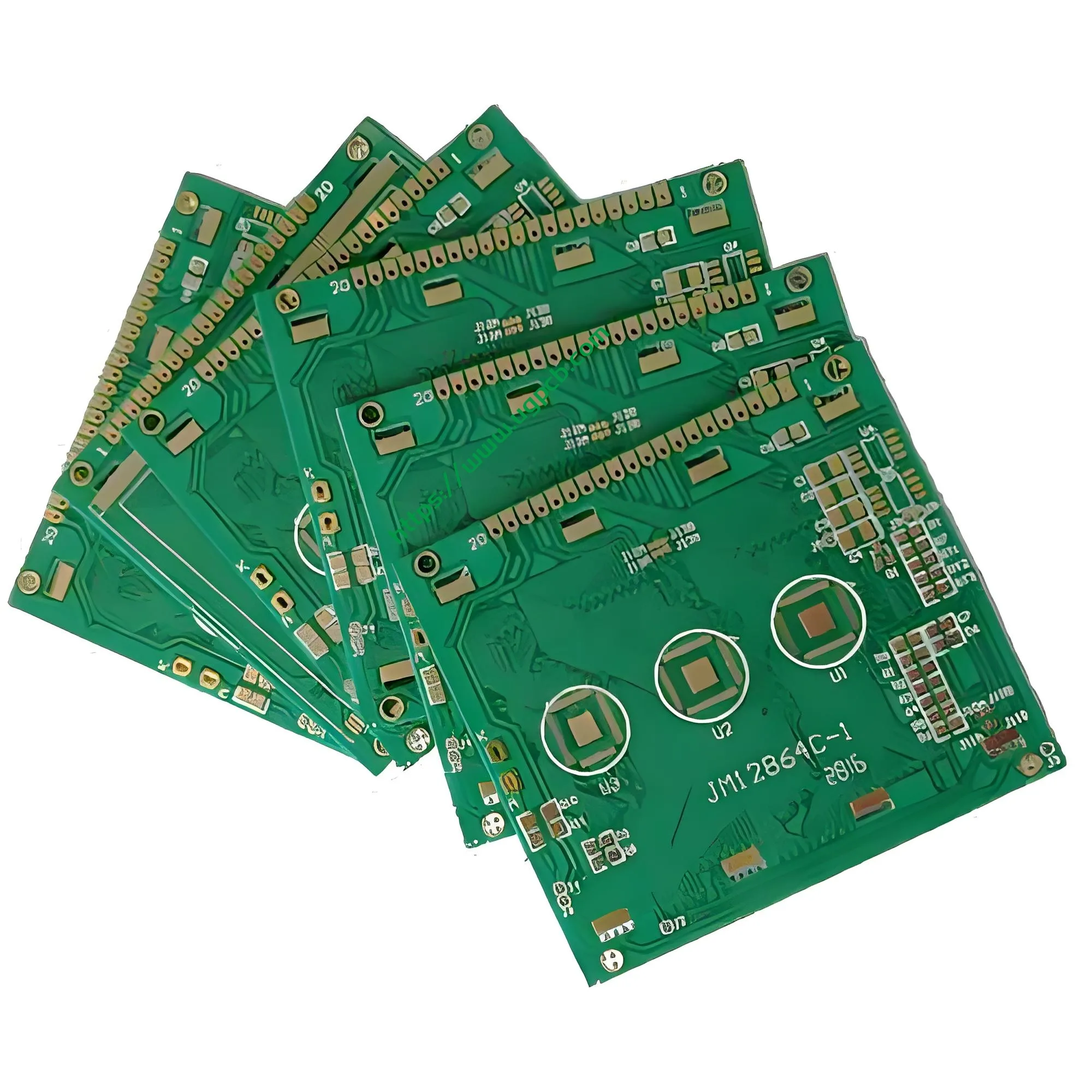
ภาพรวมผลิตภัณฑ์: โซลูชัน PCB ความน่าเชื่อถือสูงสำหรับการขับขี่จอแสดงผล LCD
UGPCB แนะนำแผงวงจร PCB จอแสดงผลคริสตัลเหลว LCD (แบบอย่าง: UGPCB-จอแอลซีดี-001), ประสิทธิภาพสูง2-แผงวงจรพิมพ์ FR-4 แบบแข็งชั้น ออกแบบมาโดยเฉพาะสำหรับการใช้งานในการขับขี่จอแสดงผลคริสตัลเหลว. ผลิตภัณฑ์นี้ใช้ลามิเนตหุ้มทองแดงคุณภาพสูง Kingboard KB6165F เป็นวัสดุฐาน, ด้วยความหนาของแผ่นกระดาน 1.6 มม. และ 1 ฟอยล์ทองแดงออนซ์ (ประมาณ 35 μm). การตกแต่งพื้นผิวใช้เห็นด้วย (นิกเกิลแบบไม่ใช้ไฟฟ้า/ทองแช่) กระบวนการที่ 2U” . คณะกรรมการมีมาตรการ 147.2 × 65 มม, โดยมีเส้นผ่านศูนย์กลางรูต่ำสุดที่ 0.22 มม. และความกว้าง/ระยะห่างบรรทัดขั้นต่ำของ 0.3 มม./0.27 มม.
นี้จอแสดงผล LCD PCB ทำหน้าที่เป็นพาหะวงจรสำคัญที่เชื่อมต่อชิปไดรเวอร์จอแสดงผลเข้ากับแผงกระจกคริสตัลเหลว. พบการใช้งานที่หลากหลายในโมดูลจอแสดงผล LCD ขนาดเล็กถึงขนาดกลาง, จอแสดงผลแผงควบคุมอุตสาหกรรม, จอแสดงผลระบบสาระบันเทิงยานยนต์, และอินเทอร์เฟซการโต้ตอบระหว่างมนุษย์กับเครื่องจักรอัจฉริยะในบ้าน.
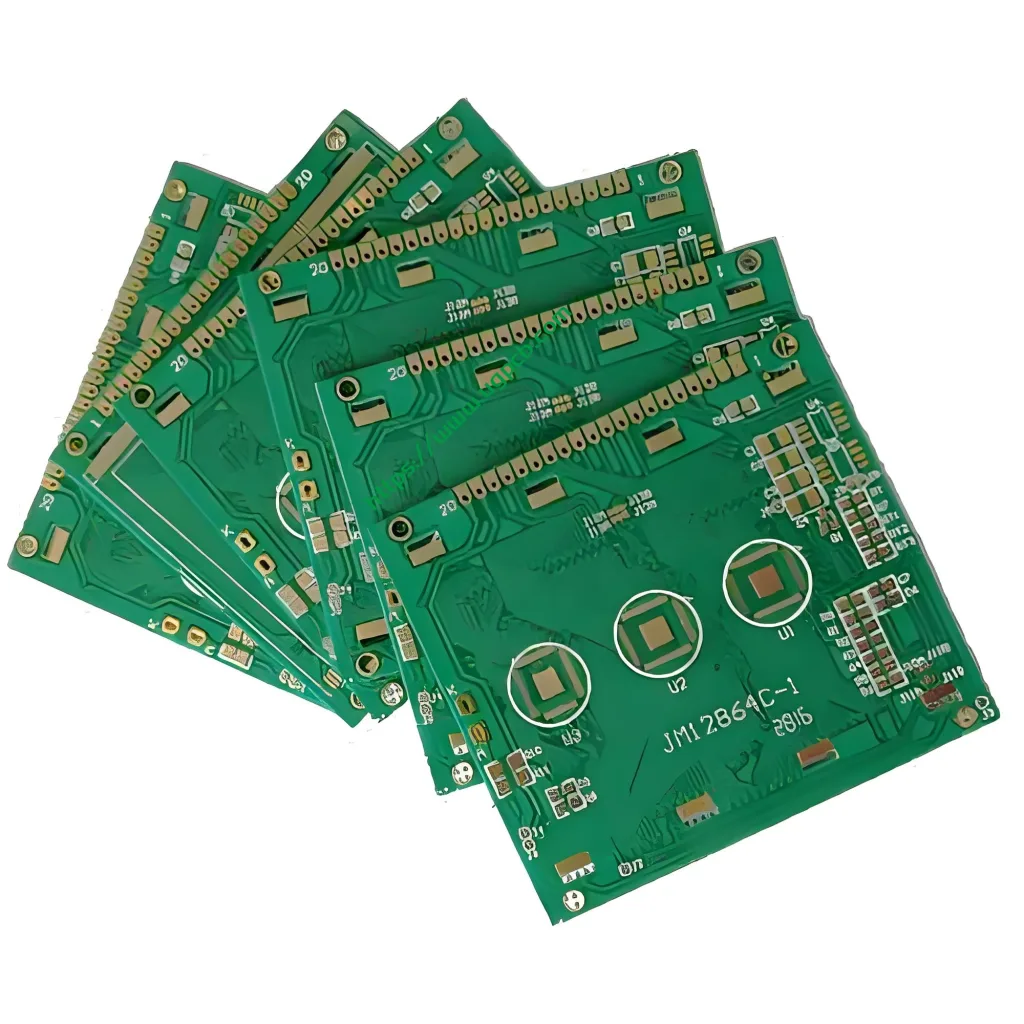
คำจำกัดความของผลิตภัณฑ์: PCB จอแสดงผลคริสตัลเหลว LCD คืออะไร?
หนึ่ง PCB จอแสดงผลคริสตัลเหลว LCD (แผงวงจรพิมพ์) เป็นแผงวงจรเฉพาะที่ออกแบบมาสำหรับระบบขับเคลื่อนจอแสดงผลคริสตัลเหลว. มันทำหน้าที่หลักสามประการ: การส่งสัญญาณการขับขี่, การกระจายพลังงาน, และการกำหนดเส้นทางสัญญาณควบคุมเวลา. ไม่เหมือนมาตรฐาน แผงวงจรพีซีบี, หนึ่ง จอแสดงผล LCD PCB ต้องการความคลาดเคลื่อนที่เข้มงวดมากขึ้นในความแม่นยำของความกว้างของเส้น, การควบคุมความต้านทาน, และความเรียบของพื้นผิว.
สินค้าชิ้นนี้เป็นของPCB สองด้านแข็ง หมวดหมู่ด้วย 2 ชั้น (2l). ใช้วัสดุทนไฟเกรด FR-4 (อล 94 วี-0 ได้รับคะแนน) และรองรับทั้ง SMT (เทคโนโลยี Mount Surface) และกระบวนการประกอบชิ้นส่วนไฮบริดผ่านรู. บอร์ดนี้มีคุณสมบัติตรงตามคลาส IPC-6012 2 ข้อกำหนดด้านประสิทธิภาพ, ทำให้เหมาะสำหรับงานอิเล็กทรอนิกส์อุตสาหกรรมและอุปกรณ์อิเล็กทรอนิกส์สำหรับผู้บริโภค.
ข้อมูลจำเพาะการออกแบบ: พารามิเตอร์ที่สำคัญสำหรับวิศวกรรม LCD PCB
วัสดุพื้นผิว: ข้อได้เปรียบ KB6165F
สินค้านี้ใช้ลามิเนตเคลือบทองแดง Kingboard KB6165F, ซึ่งมีคุณสมบัติด้านประสิทธิภาพที่สำคัญดังต่อไปนี้:
- อุณหภูมิการเปลี่ยนแก้ว (ทีจี): ≥150°ซ, รับประกันความเสถียรของมิติในระหว่างกระบวนการบัดกรีแบบรีโฟลว์ไร้สารตะกั่ว
- อุณหภูมิการสลายตัวทางความร้อน (TD): 325องศาเซลเซียส, ให้ความน่าเชื่อถือด้านความร้อนที่ดีเยี่ยม
- คะแนนความไวไฟ: อล 94 วี-0, มีเปลวไฟดับเองภายใน 10 วินาทีในการทดสอบการเผาไหม้ในแนวตั้ง
- ซีทีอี (ค่าสัมประสิทธิ์การขยายตัวทางความร้อน): 12–15 ppm/°C ในทิศทาง X-Y, 40–230 ppm/°C ในทิศทาง Z, ให้การจับคู่ระบายความร้อนที่ดีกับ IC ไดรเวอร์ LCD
- คาเฟ่ (เส้นใยขั้วบวกนำไฟฟ้า) ความต้านทาน: ประสิทธิภาพการป้องกัน CAF ที่ยอดเยี่ยมทำให้มั่นใจได้ถึงความน่าเชื่อถือในระยะยาว
- เข้ากันได้แบบไร้สารตะกั่ว: ตรงตามข้อกำหนดด้านสิ่งแวดล้อม RoHS
ตามมาตรฐานการออกแบบ IPC-2221, วัสดุที่มีค่า Tg ≥150°C เหมาะสำหรับกระบวนการประกอบแบบไร้สารตะกั่ว, สามารถรักษาความสมบูรณ์ของโครงสร้างภายใต้อุณหภูมิสูงสุดของการบัดกรีแบบรีโฟลว์ที่สูงถึง 245–260°C.
การนับเลเยอร์และการออกแบบสแต็คอัพ
คุณสมบัติของผลิตภัณฑ์ 2 ชั้น (2l) ที่มีมาตรฐาน 1.6 ความหนาของบอร์ด มม. สำหรับ IPC-2221, 1.6 มม. แสดงถึงข้อกำหนดความหนาที่ใช้บ่อยที่สุดสำหรับวัสดุแข็ง PCBS, ปรับสมดุลความแข็งแรงทางกลพร้อมความสะดวกในการประกอบ.
การออกแบบความกว้างของเส้นและระยะห่าง
ความกว้างบรรทัดขั้นต่ำของ 0.3 มม. และระยะห่างบรรทัดขั้นต่ำของ 0.27 mm เป็นพารามิเตอร์ที่เลือกสรรมาอย่างดีสำหรับจอแอลซีดีไดรเวอร์ PCB ความสมบูรณ์ของสัญญาณ. ภายใต้มาตรฐาน IPC-2221, ข้อกำหนดระยะห่างขั้นต่ำสำหรับแรงดันไฟฟ้าทั่วไป (≤30V) การติดตามสัญญาณดิจิตอลคือ 0.1 มม (4 MIL). สินค้าชิ้นนี้ 0.27 มม (ประมาณ 10.6 MIL) ระยะห่างเกินข้อกำหนดขั้นต่ำของ IPC, ให้อัตรากำไรที่เพียงพอสำหรับคุณภาพสัญญาณ.
การอ้างอิงการคำนวณการออกแบบ (ขึ้นอยู่กับสูตรแบบง่ายของความสามารถในการรับกระแสไฟฟ้าของตัวนำชั้นนอก IPC-2221):
ความสามารถในการรับกระแสไฟของชั้นนอก asym k × ΔT^0.448 × W^0.725 × T^0.725
โดยที่ k = 0.048 (สำหรับชั้นนอก). ที่อุณหภูมิเพิ่มขึ้น 10°C, อัน 0.3 มม. ติดตามด้วย 1 ความหนาของทองแดงออนซ์ให้ความสามารถในการจ่ายกระแสไฟฟ้าตามทฤษฎีประมาณ 1.2–1.5 A ซึ่งเพียงพอสำหรับข้อกำหนดด้านพลังงานและการติดตามสัญญาณของบอร์ดไดรเวอร์ LCD ทั่วไป.
เส้นผ่านศูนย์กลางรูขั้นต่ำ
เส้นผ่านศูนย์กลางรูขั้นต่ำของ 0.22 มม (ประมาณ 8.7 MIL) จัดอยู่ในหมวดการเจาะที่แม่นยำ. ภายใต้ IPC-6012, ความคลาดเคลื่อนของเส้นผ่านศูนย์กลางรูเจาะมาตรฐานคือ ±0.08 มม (ประมาณ ±3 ล้าน) . สำหรับ 0.22 มม. ไมโครเวียส, โดยทั่วไปความคลาดเคลื่อนในการผลิตจะถูกควบคุมภายใน ± 0.05 มม.
พื้นผิวเสร็จสิ้น: เห็นด้วย 2U”
ที่เห็นด้วย (นิกเกิลแบบไม่ใช้ไฟฟ้า/ทองแช่) เคลือบผิวด้วย 2U” ความหนาของทองคำ (ประมาณ 0.05 μm) เป็นไปตามข้อกำหนด IPC-4552. IPC-4552 การแก้ไข A (ออกใน 2017) ระบุความหนาของชั้นสะสมทองคำของ 0.04 ไมโครเมตรถึง 0.10 μm (1.6 μinถึง 4.0 นาที) และความหนาของนิกเกิล 3 ไมโครเมตรถึง 6 μm.
ข้อดีของการตกแต่งพื้นผิว ENIG:
- ความสามารถในการบัดกรีที่ดีเยี่ยม รองรับรอบการรีโฟลว์หลายรอบ
- ความสามารถในการเชื่อมลวดที่แข็งแกร่ง
- ต้านทานการเกิดออกซิเดชันและการกัดกร่อนที่เหนือกว่า
- พื้นผิวเรียบเหมาะสำหรับการติดตั้งส่วนประกอบที่มีระยะพิทช์ละเอียด
- อายุการเก็บรักษาที่ยาวนานขึ้น
หลักการทำงาน: กลไกการส่งสัญญาณของ PCB จอแสดงผล LCD
ที่จอแสดงผลคริสตัลเหลว LCD PCB ทำงานในสองหน้าที่หลัก: การส่งสัญญาณ และการกระจายพลังงาน.
1. จอแสดงผลการส่งสัญญาณของไดรเวอร์: แสดงข้อมูลจากชิปควบคุมหลัก (มจร/SoC) เดินทางผ่านแผงวงจรพีซีบี ผ่านไมโครสตริปหรือแถบลายเส้นไปยัง IC ไดรเวอร์ LCD. IC ไดรเวอร์จะแปลงสัญญาณดิจิตอลเป็นแรงดันไฟฟ้าระดับสีเทาแบบอะนาล็อก, ซึ่งจะถูกส่งออกผ่านทางพีซีบีมีรอยละเอียดของอิเล็กโทรด ITO บนแผงกระจกคริสตัลเหลว, ควบคุมมุมบิดของโมเลกุลคริสตัลเหลวเพื่อสร้างภาพที่แสดง.
2. การกำหนดเส้นทางสัญญาณควบคุมเวลา: ที่จอแสดงผล LCD PCB นำสัญญาณจังหวะที่สำคัญรวมถึง VSYNC (ซิงค์แนวตั้ง), เอชซิงค์ (ซิงค์แนวนอน), ดีซีแอลเค (นาฬิกาพิกเซล), และ DE (เปิดใช้งานข้อมูล). ความล่าช้าในการส่งและการจับคู่อิมพีแดนซ์ของสัญญาณเหล่านี้ส่งผลโดยตรงต่อคุณภาพการแสดงผล.
3. การกระจายการจัดการพลังงาน: ที่แผงวงจรแอลซีดี แปลงกำลังไฟฟ้าเข้า (โดยทั่วไป 3.3 วีหรือ 5 วี) ผ่านวงจรแปลง DC-DC เพื่อสร้างระดับแรงดันไฟฟ้าหลายระดับที่แผง LCD ต้องการ, รวมทั้งวีจีเอชด้วย (แรงดันไฟเข้าประตู, โดยทั่วไป +15 วีถึง +30 วี), อ้างอิง (แรงดันไฟฟ้าเกตออฟ, โดยทั่วไป −5 V ถึง −15 V), และ AVDD (แรงดันไฟฟ้าแบบอะนาล็อก).
การจำแนกประเภทผลิตภัณฑ์: หมวดหมู่ PCB จอแอลซีดี
PCB จอแสดงผลคริสตัลเหลว LCD สามารถจำแนกได้ตามมิติต่างๆ ดังต่อไปนี้:
โดยการนับเลเยอร์
- กระดานด้านเดียว: ใช้สำหรับจอแสดงผล LCD แบบแบ่งส่วนอย่างง่าย
- กระดานสองด้าน (2l): หมวดหมู่ของผลิตภัณฑ์นี้, ใช้สำหรับไดรเวอร์จอแสดงผล TFT-LCD ขนาดเล็กถึงขนาดกลาง
- บอร์ดหลายชั้น (4L และสูงกว่า): ใช้สำหรับความละเอียดสูง, โมดูลแสดงผลขนาดใหญ่
โดยพื้นผิวเสร็จสิ้น
- บอร์ดอีนิก: หมวดหมู่ของผลิตภัณฑ์นี้, นำเสนอประสิทธิภาพโดยรวมที่ดีที่สุด
- บอร์ด OSP: ต้นทุนที่ต่ำกว่า, เหมาะสำหรับอุปกรณ์อิเล็กทรอนิกส์สำหรับผู้บริโภคที่มีวงจรชีวิตสั้น
- บอร์ด HASL: เหมาะสำหรับบอร์ดไดรเวอร์ LCD ที่มีพินพินกว้างขึ้น
โดยการสมัคร
- เครื่องใช้ไฟฟ้า LCD PCB: จอแสดงผลรองของสมาร์ทโฟน, สมาร์ทวอทช์แสดง, หน้าจอ e-reader
- PCB จอแอลซีดีควบคุมอุตสาหกรรม: HMI อุตสาหกรรม, แผงหน้าปัดแสดง, ไดรเวอร์จอแสดงผลแผงควบคุมการทำงานของ CNC
- PCB จอแอลซีดีสำหรับยานยนต์: ระบบสาระบันเทิงภายในรถยนต์, แผงหน้าปัดดิจิตอล, แผงควบคุมการแสดงผล HUD
- PCB จอแอลซีดีอุปกรณ์การแพทย์: จอภาพผู้ป่วย, อุปกรณ์วินิจฉัยอัลตราซาวนด์, บอร์ดควบคุมจอแสดงผลระบบภาพทางการแพทย์
ข้อมูลจำเพาะด้านประสิทธิภาพหลัก
| พารามิเตอร์ | ข้อมูลจำเพาะ | มาตรฐานอ้างอิง |
|---|---|---|
| วัสดุลามิเนต | KB6165F (คิงบอร์ด) | - |
| ประเภทลามิเนต | FR-4 ผ้าแก้วเคลือบทองแดงลามิเนต | อล 94 วี-0 |
| จำนวนเลเยอร์ | 2 ชั้น (2l) | - |
| ความหนาของบอร์ด | 1.6 มม | ไอพีซี-2221 |
| ความหนาของทองแดงชั้นนอก | 1 ออนซ์ (35 μm) | IPC-6012 คลาส 2 |
| พื้นผิวเสร็จสิ้น | เพียง 2U” (0.05 ไมโครเมตร) | ไอพีซี-4552 |
| ความหนาของชั้นนิกเกิล | 3–6 ไมโครเมตร (ชั้นล่าง) | IPC-4552 Rev A |
| เส้นผ่านศูนย์กลางรูขั้นต่ำ | 0.22 มม | ไอพีซี-6012 |
| ความกว้างบรรทัดขั้นต่ำ | 0.3 มม | ไอพีซี-2221 |
| ระยะห่างระหว่างบรรทัดขั้นต่ำ | 0.27 มม | ไอพีซี-2221 |
| ขนาดบอร์ด | 147.2 × 65 มม | - |
| ทีจี (อุณหภูมิการเปลี่ยนแก้ว) | ≥150°ซ | - |
| TD (อุณหภูมิการสลายตัวทางความร้อน) | 325องศาเซลเซียส | - |
| ซีทีอี (ทิศทาง X-Y) | 12–15 ppm/°C | - |
| คะแนนความไวไฟ | อล 94 วี-0 | มาตรฐาน UL94 |
| ความต้านทานส่วนโค้ง | ≥60วินาที | - |
| ความต้านทานพื้นผิว | ≥2.6 × 10⁸ MΩ | - |
| ความต้านทานระดับเสียง | ≥3.4 × 10⁹ MΩ·ซม | - |
การวิเคราะห์โครงสร้างผลิตภัณฑ์
ที่จอแสดงผลคริสตัลเหลว LCD PCB โครงสร้างประกอบด้วยชั้นต่อไปนี้จากภายนอกสู่ภายใน:
1. ชั้นนอก – พื้นผิว ENIG: ชั้นทองที่ 2U” (ประมาณ 0.05 μm) ปกป้องชั้นนิกเกิลที่อยู่ด้านล่างจากการเกิดออกซิเดชัน. ชั้นนิกเกิลด้านล่างที่ 3–6 ไมโครเมตร ทำหน้าที่เป็นตัวกั้นการแพร่กระจายระหว่างทองแดงและทองคำ.
2. ชั้นฟอยล์ทองแดง: 1 ออนซ์ (ประมาณ 35 μm) ฟอยล์ทองแดงที่ติดด้วยไฟฟ้า, นำมาแกะสลักเป็นลวดลายวงจร.
3. ชั้นอิเล็กทริก: ผ้าแก้วเกรด FR-4 ชุบด้วยอีพอกซีเรซิน, ประมาณ 0.7 หนา มม (ชั้นเดียว), ให้ฉนวนไฟฟ้าและการสนับสนุนทางกล.
4. ชั้นฟอยล์ทองแดง: ชั้นล่าง 1 ทองแดงออนซ์สร้างรูปแบบวงจรด้านล่าง.
5. ชั้นนอก – พื้นผิว ENIG: การรักษาด้วย ENIG แบบสมมาตรที่เข้าคู่กับชั้นบนสุด.
คุณสมบัติผลิตภัณฑ์: เหตุใดจึงเลือก PCB จอแสดงผล LCD ของ UGPCB?
1 การผลิตที่มีความแม่นยำสูง: เส้นผ่านศูนย์กลางรูขั้นต่ำของ 0.22 มม. และความกว้าง/ระยะห่างบรรทัดขั้นต่ำของ 0.3 มม./0.27 มม. รองรับข้อกำหนดการกำหนดเส้นทางของบอร์ดไดรเวอร์ LCD ความหนาแน่นสูง.
② วัสดุพื้นผิวระดับพรีเมี่ยม: Kingboard KB6165F วัสดุ FR-4 ระดับไฮเอนด์ที่มี Tg ≥150°C และ UL 94 วี-0 ระดับการติดไฟช่วยให้มั่นใจถึงความเข้ากันได้ของกระบวนการไร้สารตะกั่วและความน่าเชื่อถือในระยะยาว.
3. พื้นผิวที่ได้มาตรฐาน: เพียง 2U” กระบวนการสอดคล้องกับ IPC-4552, ให้ความสามารถในการบัดกรีที่ดีเยี่ยม, ความต้านทานต่อการเกิดออกซิเดชัน, และอายุการเก็บรักษาที่ยาวนานขึ้น.
④ การควบคุมคุณภาพอย่างเข้มงวด: ผลิตภัณฑ์ได้รับการควบคุมคุณภาพทุกกระบวนการตามคลาส IPC-6012 2 มาตรฐาน, ครอบคลุมความทนทานต่อเส้นผ่านศูนย์กลางรู (±0.08 มม), ความหนาของทองแดงรู (≥20 ไมโครเมตร), ความสมบูรณ์ของหน้ากากประสาน, และการทดสอบทางไฟฟ้า.
⑤ การออกแบบที่ปรับให้เหมาะสมกับ LCD: การควบคุมความต้านทาน, ความสมบูรณ์ของสัญญาณ, และความสมบูรณ์ของพลังงานได้รับการปรับให้เหมาะสมโดยเฉพาะสำหรับการใช้งานในการขับขี่จอแสดงผลคริสตัลเหลว.
กระบวนการผลิต: จากวัตถุดิบสู่ผลิตภัณฑ์สำเร็จรูป
UGPCB ปฏิบัติตามกระบวนการผลิตมาตรฐานที่เข้มงวดสำหรับPCB จอแสดงผล LCD:
1. การตัดวัสดุ →2. การถ่ายโอนรูปแบบเลเยอร์ภายใน (เครื่องหมายระบุตำแหน่งการเจาะและการลงทะเบียน) →3. การขุดเจาะ (เส้นผ่านศูนย์กลางรูขั้นต่ำ 0.22 มม. ± 0.08 มม) →4. การสะสมทองแดงแบบไม่ใช้ไฟฟ้า/การชุบด้วยไฟฟ้า (การทำให้เป็นโลหะของรู, ความหนาของทองแดงรู≥20μm) →5. การถ่ายโอนรูปแบบชั้นนอก (ความกว้างของเส้น 0.3 มม / ระยะห่าง 0.27 มม) →6. การชุบลวดลาย (ทองแดงสะสมถึง 1 ออนซ์) →7. การแกะสลัก →8. การพิมพ์หน้ากากประสาน →9. ENIG พื้นผิวสำเร็จรูป (เห็นด้วย, ทองหนา 2U”) →10. การทำโปรไฟล์ (ขนาด 147.2 × 65 มม) →11. การทดสอบไฟฟ้า (100% การทดสอบทางไฟฟ้า) →12. การตรวจสอบขั้นสุดท้าย (Aoi + การตรวจสอบด้วยสายตา) →13. บรรจุภัณฑ์และการจัดส่ง
สถานการณ์แอปพลิเคชันทั่วไป
📱 เครื่องใช้ไฟฟ้า: จอแสดงผลรองของสมาร์ทโฟน, สมาร์ทวอทช์แสดง, PCB ไดรเวอร์หน้าจอ e-reader.
🏭 การควบคุมอุตสาหกรรม: อินเทอร์เฟซระหว่างมนุษย์และเครื่องจักร PLC (เอชเอ็มไอ), การแสดงเครื่องมืออุตสาหกรรม, แผงไดรเวอร์จอแสดงผลแผงควบคุมการทำงานของ CNC.
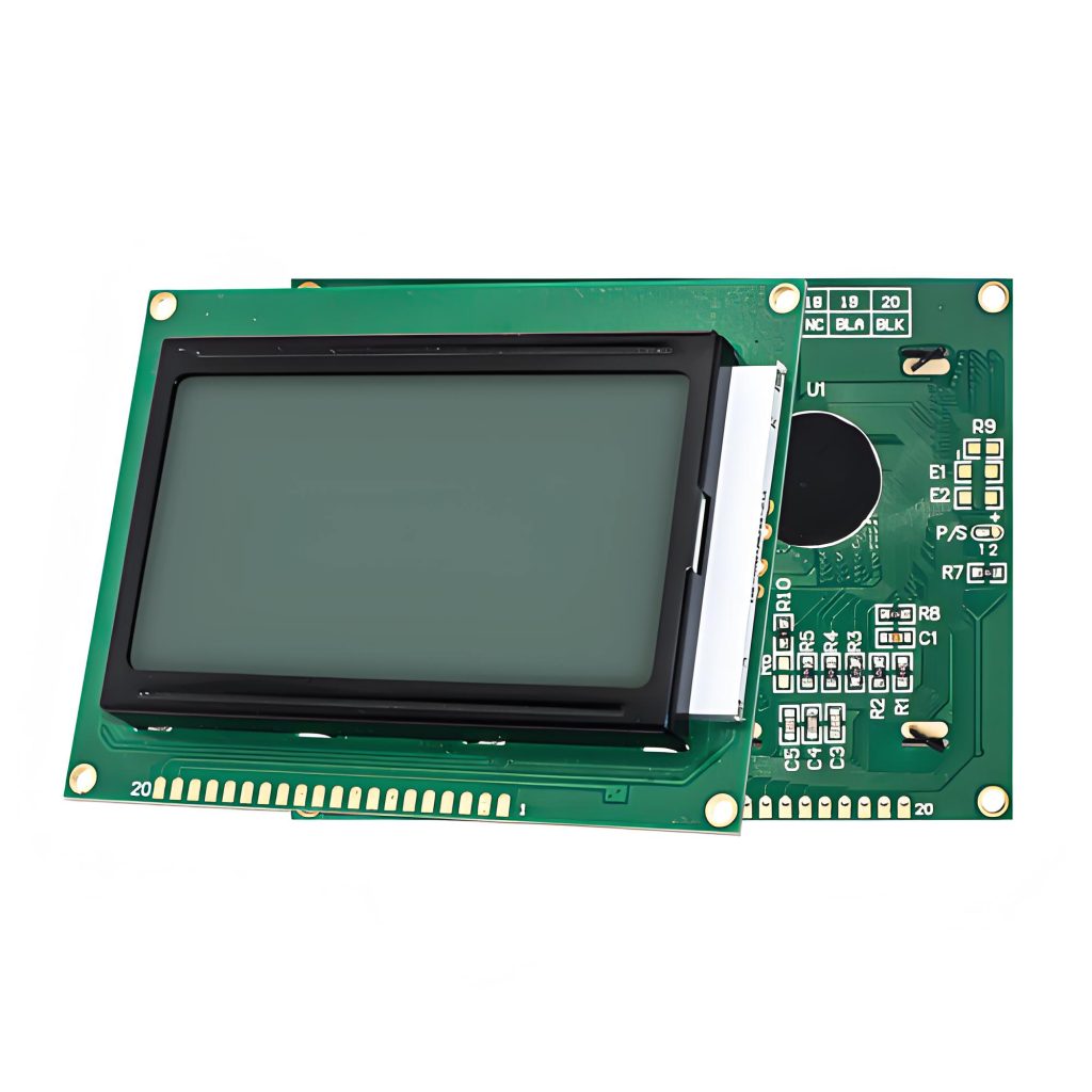
🚗 เครื่องใช้ไฟฟ้าในรถยนต์: ระบบสาระบันเทิงภายในรถยนต์, แผงหน้าปัดดิจิตอล, จอแสดงผลบนศีรษะ (ฮัด) PCB ควบคุมการแสดงผล.
🏥 อุปกรณ์การแพทย์: จอภาพผู้ป่วย, อุปกรณ์วินิจฉัยอัลตราซาวนด์, แผงวงจรควบคุมระบบภาพทางการแพทย์.
🏠 สมาร์ทโฮม: ระบบควบคุมการเข้าออกอัจฉริยะแสดงขึ้น, แผงควบคุมอุปกรณ์อัจฉริยะ, อาคารโมดูลแสดงผลระบบอินเตอร์คอม PCBs.
ทำไมต้องเลือก UGPCB?
UGPCB นำปีแห่ง จอแสดงผล LCD PCB ประสบการณ์การผลิตให้กับทุกโครงการ. เราใช้วัตถุดิบพรีเมี่ยมอย่าง Kingboard KB6165F, บังคับใช้คลาส IPC-6012 อย่างเคร่งครัด 2 มาตรฐานคุณภาพ, และใช้งานอุปกรณ์เจาะและทำลวดลายวงจรที่มีความแม่นยำสูง. ไม่ว่าคุณจะต้องการ จอแอลซีดี PCB Prototyping หรือปริมาณการผลิต, UGPCB ให้ความแม่นยำสูง, โซลูชันผลิตภัณฑ์ที่มีความน่าเชื่อถือสูง.
📞 รับโซลูชัน PCB จอแสดงผล LCD เลยวันนี้
UGPCB PCB จอแสดงผลคริสตัลเหลว LCD ได้รับการนำไปใช้อย่างประสบความสำเร็จในอุตสาหกรรมต่างๆ มากมาย, ยานยนต์, และโครงการจัดแสดงสินค้าอิเล็กทรอนิกส์สำหรับผู้บริโภค. ไม่ว่าคุณจะต้องการ การสร้างต้นแบบ PCB จอแอลซีดี เพื่อการตรวจสอบการออกแบบหรือ พีซีบี บริการประกอบกุญแจแบบครบวงจร, UGPCB ให้การสนับสนุนกระบวนการเต็มรูปแบบตั้งแต่การผลิต PCB ไปจนถึง พีซีบี แอสเซมบลี SMT.
ติดต่อทีมงานมืออาชีพของ UGPCB วันนี้เพื่อรับโซลูชัน PCB จอแสดงผล LCD แบบกำหนดเองของคุณ!
📧 อีเมล: [info@ugpcb.com]
📞 โทรศัพท์: [+86-755-XXXXXXXXX]
🌐 เว็บไซต์: [www.ugpcb.com]
การระบุแหล่งที่มาของข้อมูล
มาตรฐานทางเทคนิคและข้อมูลที่อ้างถึงในเอกสารนี้ได้มาจากแหล่งข้อมูลที่เชื่อถือได้ดังต่อไปนี้:
- ไอพีซี-6012 -ข้อกำหนดคุณสมบัติและประสิทธิภาพสำหรับบอร์ดพิมพ์แข็ง – กำหนดความคลาดเคลื่อนของเส้นผ่านศูนย์กลางรู PCB (มาตรฐาน ±0.08 มม), ความหนาของทองแดงรู (ระดับ 2 ≥20 ไมโครเมตร), และข้อกำหนดระดับประสิทธิภาพ
- ไอพีซี-2221 -มาตรฐานทั่วไปเกี่ยวกับการออกแบบแผ่นพิมพ์ – ระบุข้อกำหนดการออกแบบความกว้างของเส้น/ระยะห่าง และสูตรการคำนวณกำลังการผลิตปัจจุบัน
- IPC-4552 การแก้ไข A (ออกแล้ว 2017) -ข้อกำหนดด้านประสิทธิภาพสำหรับนิกเกิลแบบไม่ใช้ไฟฟ้า/ทองแช่ (เห็นด้วย) การชุบสำหรับบอร์ดพิมพ์ – ระบุข้อกำหนดความหนาของชั้นฝากของ ENIG: นิกเกิล 3–6 ไมโครเมตร, ทอง 0.04–0.10 ไมโครเมตร
- อล 94 -มาตรฐานความปลอดภัยความไวไฟของวัสดุพลาสติกสำหรับชิ้นส่วนในอุปกรณ์และเครื่องใช้ – วี-0 การให้คะแนนต้องใช้เปลวไฟดับเองภายใน 10 ไม่กี่วินาที
- เอกสารข้อมูลผลิตภัณฑ์ Kingboard KB6165F – พารามิเตอร์ทางเทคนิคของพื้นผิว (Tg ≥150°C, อุณหภูมิ 325°C, อล 94 วี-0, ฯลฯ)
- กิกะไบต์/ที 4677 -วิธีทดสอบสำหรับบอร์ดแบบพิมพ์ – ใช้ร่วมกับมาตรฐาน IPC เพื่อใช้อ้างอิงการตรวจสอบ













