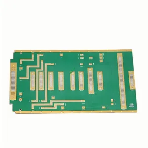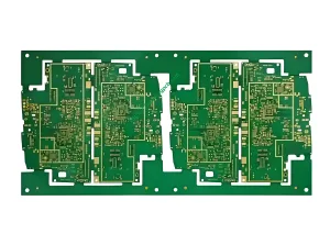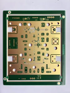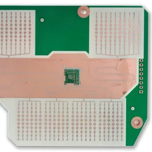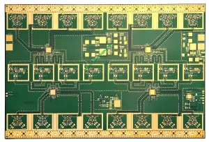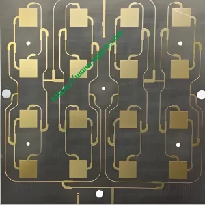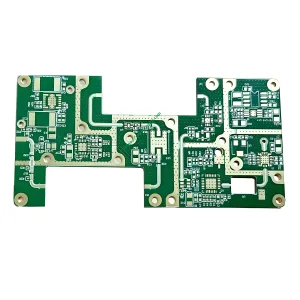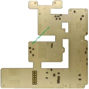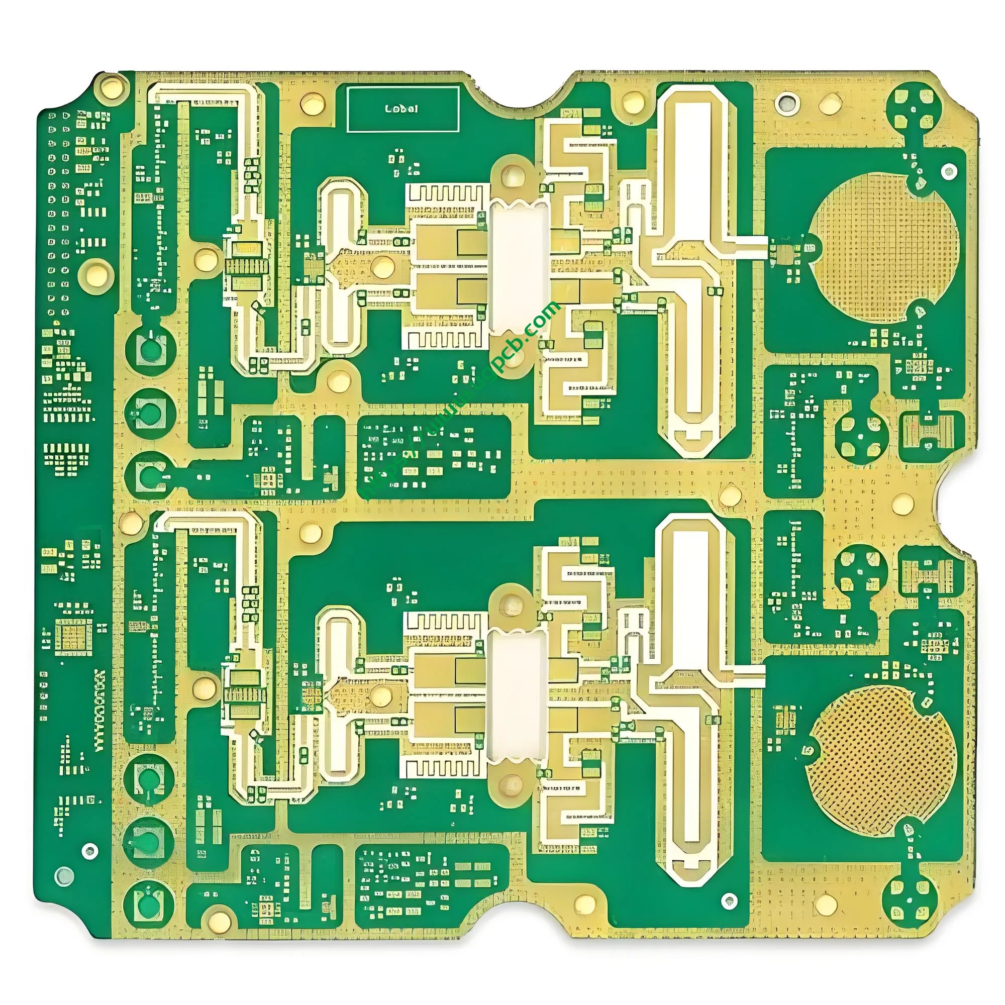
ภาพรวมผลิตภัณฑ์
บอร์ด PCB Lightwave Communications เป็นแผงบังตาไฮบริด 6 ชั้นประสิทธิภาพสูงที่ฝังไว้ผ่านแผงวงจรพิมพ์ที่ออกแบบโดย UGPCB สำหรับการสื่อสารแบบออปติกและการส่งสัญญาณดิจิทัลความเร็วสูง. ผลิตภัณฑ์นี้มีการรวมสแต็คอัพแบบไฮบริดวัสดุดิจิทัลความเร็วสูง TU872 กับวัสดุความถี่สูง Rogers RO4350B. การออกแบบผสานความสามารถในการประมวลผลสัญญาณดิจิตอลความเร็วสูงเข้ากับประสิทธิภาพการส่งสัญญาณ RF และไมโครเวฟที่ยอดเยี่ยม. PCB นี้ทำหน้าที่เป็นโซลูชันการเชื่อมต่อระหว่างกันในอุดมคติสำหรับอุปกรณ์รับสัญญาณกราวด์การสื่อสารด้วยแสง, ตัวรับส่งสัญญาณแสงความเร็วสูง, และโมดูลส่วนหน้า RF ของสถานีฐาน.
ที่ พีซีบี อุตสาหกรรมยังคงผลักดันไปสู่ความถี่ที่สูงขึ้น, ความเร็วที่เร็วขึ้น, และมีความหนาแน่นมากขึ้น. โซลูชันวัสดุเดี่ยวไม่สามารถตอบสนองความต้องการที่ขัดแย้งกันของสัญญาณดิจิตอลความเร็วสูงและสัญญาณอะนาล็อก RF ได้อีกต่อไป. UGPCB จัดการกับความท้าทายนี้ผ่านการออกแบบไฮบริด TU872+RO4350B. PCB 6 เลเยอร์นี้ให้ความสมดุลที่เหมาะสมระหว่างความสมบูรณ์ของสัญญาณ, การจัดการความร้อน, และต้นทุนการผลิต.

การจำแนกประเภทผลิตภัณฑ์
ต่อ IPC-6012Eข้อกำหนดคุณสมบัติและประสิทธิภาพสำหรับบอร์ดพิมพ์แข็ง, ผลิตภัณฑ์นี้จัดอยู่ในประเภทต่อไปนี้:
| มิติการจำแนกประเภท | หมวดหมู่ |
|---|---|
| ประเภทโครงสร้าง | กระดานพิมพ์แข็งหลายชั้น (6 ชั้น) ด้วยจุดอ่อนที่ตาบอดและถูกฝังไว้ |
| ระบบวัสดุ | ไฮบริดลามิเนต (วัสดุดิจิทัลความเร็วสูง + วัสดุความถี่สูง) |
| พื้นผิวเสร็จสิ้น | นิกเกิลแบบไม่ใช้ไฟฟ้า/ทองแช่ (เห็นด้วย), สำหรับ IPC-4552 |
| ระดับความน่าเชื่อถือ | ตรงตามคลาส IPC-6012 2 (บริการเฉพาะผลิตภัณฑ์อิเล็กทรอนิกส์) และชั้นเรียน 3 (ผลิตภัณฑ์อิเล็กทรอนิกส์ที่น่าเชื่อถือสูง) ความต้องการ |
| คะแนนความไวไฟ | อล 94 วี-0 |
| โดเมนแอปพลิเคชัน | การสื่อสารด้วยแสง / PCB โครงสร้างพื้นฐานโทรคมนาคม |
ข้อมูลจำเพาะทางเทคนิคหลัก
| พารามิเตอร์ | ข้อมูลจำเพาะ |
|---|---|
| เลเยอร์ | 6 ชั้น |
| วัสดุ | Tu872 (เลเยอร์ดิจิทัลความเร็วสูง) + RO4350B (ชั้นความถี่สูง) |
| ความหนาของบอร์ด | 1.8 มม |
| ความหนาของทองแดง | 35/35/35/35 μm (กระจายสม่ำเสมอทั่วทุกชั้น) |
| เส้นผ่านศูนย์กลางรูเล็กที่สุด | 0.20 มม |
| การรักษาพื้นผิว | เห็นด้วย (2คุณ” ความหนาของทองคำ) |
| คุณสมบัติทางเทคนิค | การเสียบสูญญากาศ + จุดแวะตาบอดและฝังอยู่ |
คุณสมบัติของวัสดุหลัก
Rogers RO4350B วัสดุความถี่สูง (สำหรับชั้นสัญญาณ RF/ไมโครเวฟ):
- ค่าคงที่ไดอิเล็กตริก (ดีเค): 3.48 ± 0.05 @ 10 กิกะเฮิรตซ์
- ปัจจัยการกระจาย (ฟ): 0.0037 @ 10 กิกะเฮิรตซ์
- ค่าสัมประสิทธิ์การขยายตัวทางความร้อนของแกน Z (ซีทีอี): 32 ppm/° C
- คะแนนความไวไฟ: อล 94 วี-0
- การนำความร้อน: 0.69 w/(M · K)
วัสดุดิจิทัลความเร็วสูง TU872 (สำหรับชั้นสัญญาณดิจิตอลความเร็วสูง):
- ค่าคงที่ไดอิเล็กตริก (ดีเค): < 3.5 @ 10 กิกะเฮิรตซ์
- ปัจจัยการกระจาย (ฟ): ~0.009 @ 10 กิกะเฮิรตซ์
- อุณหภูมิการเปลี่ยนสถานะคล้ายแก้วสูง (ทีจี) มีเสถียรภาพทางความร้อนที่ดีเยี่ยมและต้านทาน CAF
แนวทางการออกแบบ
สถาปัตยกรรมสแต็คอัพแบบไฮบริด
PCB 6 เลเยอร์นี้ใช้การซ้อนกันแบบไฮบริดด้วยวัสดุ TU872 และ RO4350B. ตำแหน่งหลักการออกแบบหลักRO4350B บนชั้นนอกหรือชั้นสัญญาณเฉพาะที่ต้องการการส่งสัญญาณ RF ความถี่สูง, ในขณะที่TU872 ให้บริการเลเยอร์การประมวลผลสัญญาณดิจิตอลความเร็วสูง. การจัดสรรวัสดุเชิงกลยุทธ์นี้ทำให้ PCB ตัวเดียวสามารถจัดการทั้งสัญญาณ RF ระดับ GHz และสัญญาณลอจิกดิจิทัลความเร็วสูง, ขจัดการประนีประนอมด้านประสิทธิภาพที่มีอยู่ในโซลูชันวัสดุเดี่ยว.
คนตาบอดและถูกฝังด้วยการออกแบบ
Blind Vias เชื่อมต่อชั้นนอกกับชั้นในโดยไม่เจาะความหนาของบอร์ดทั้งหมด. จุดแวะที่ฝังอยู่ทั้งหมดภายในกระดาน, มองไม่เห็นจากพื้นผิวด้านนอกทั้งสองข้าง. PCB 6 เลเยอร์นี้ใช้ประโยชน์จากเทคโนโลยีที่มองไม่เห็นและฝังไว้เพื่อให้ได้ความหนาแน่นของการกำหนดเส้นทางระดับ HDI.
ต่อ IPC-6012E, บอร์ดหลายชั้น ที่มีจุดซ่อนเร้นและฝังต้องเป็นไปตามข้อกำหนดการชุบและการเติมที่เข้มงวด. ที่ 0.20 เส้นผ่านศูนย์กลางรูขั้นต่ำ มม. ช่วยให้ผลผลิตการผลิตสมดุลด้วยความสามารถในการกำหนดเส้นทางที่มีความหนาแน่นสูง. ในกระดาน 6 ชั้น, Blind Vias จากชั้นนอกไปยังชั้นในจำเป็นต้องมีการควบคุมเชิงลึกที่แม่นยำ—พวกมันจะต้องเจาะไปยังชั้นในเป้าหมายโดยไม่ทำลายวงจรชั้นใน, โดยยังคงรักษาพื้นที่การเชื่อมต่อให้เพียงพอ.
การออกแบบการควบคุมอิมพีแดนซ์
อิมพีแดนซ์ลักษณะเฉพาะของสายส่งสัญญาณเป็นไปตามสูตรนี้ (โครงสร้างไมโครสตริป):
ที่ไหน เป็นค่าคงที่ไดอิเล็กตริก, คือความหนาอิเล็กทริก, คือความกว้างของรอยเส้น, และ คือความหนาของทองแดง. ค่าเผื่อ Dk ที่แน่นหนาของ RO4350B ที่ ±0.05 รับประกันความเบี่ยงเบนน้อยที่สุดระหว่างค่าความต้านทานที่ออกแบบและประดิษฐ์. ความแม่นยำนี้พิสูจน์ได้ว่ามีความสำคัญอย่างยิ่งต่อการควบคุมอิมพีแดนซ์แบบปลายเดี่ยว 50Ω หรือดิฟเฟอเรนเชียล 100Ω ในอุปกรณ์สื่อสารด้วยแสงที่แม่นยำ.
หลักการปฏิบัติงาน
หลักการส่งสัญญาณ
ที่ความถี่สูง, สายส่งสัญญาณ PCB ทำหน้าที่เป็นสายส่งพารามิเตอร์แบบกระจาย. ค่าคงที่ไดอิเล็กทริก (ดีเค) ของวัสดุพื้นผิวจะกำหนดความเร็วการแพร่กระจายของสัญญาณ:
ที่ไหน คือความเร็วแสงในสุญญากาศ (3×10⁸ เมตร/วินาที) และ คือค่าคงที่ไดอิเล็กทริกที่มีประสิทธิผล. ค่า Dk ต่ำของ RO4350B (3.48) ช่วยให้สามารถกระจายสัญญาณได้ประมาณ 54% ความเร็วแสงในสุญญากาศ ซึ่งเร็วกว่าวัสดุ FR-4 ทั่วไปอย่างมาก (ดเค µ 4.2-4.8).
กลไกการสูญเสีย
การสูญเสียสัญญาณทั้งหมดในสายส่ง PCB ประกอบด้วยการสูญเสียตัวนำ และการสูญเสียอิเล็กทริก. การสูญเสียอิเล็กทริกมีความสัมพันธ์โดยตรงกับปัจจัยการกระจายตัวของวัสดุ (ฟ):
ที่ไหน คือความถี่สัญญาณและ คือ Df. Df ของ RO4350B เพียงเท่านั้น 0.0037 ที่ 10 GHz ให้การสูญเสียอิเล็กทริกต่ำมากต่อความยาวหน่วย. คุณลักษณะนี้พิสูจน์ให้เห็นถึงความจำเป็นสำหรับสัญญาณการสื่อสารแบบออปติกที่ทำงานที่ความถี่ข้างต้น 10 กิกะเฮิรตซ์.
คนตาบอดและฝังผ่านการเชื่อมต่อไฟฟ้า
จุดซ่อนเร้นและฝังไว้จะสร้างการเชื่อมต่อในแนวตั้งระหว่างชั้นเฉพาะภายใน PCB 6 ชั้นที่ซ้อนกัน. เมื่อเทียบกับจุดผ่านรูทะลุ, ช่วยลดความจุของปรสิตและผลกระทบจากการเหนี่ยวนำที่ทำให้ความสมบูรณ์ของสัญญาณความเร็วสูงลดลงอย่างมาก. การลดผลกระทบของปรสิตนี้มีผลกระทบอย่างชัดเจนต่อการรักษาความสมบูรณ์ของสัญญาณสำหรับสัญญาณดิจิตอลและ RF ความเร็วสูง.
กระบวนการผลิต
การเตรียมลามิเนตไฮบริด
การซ้อนกันแบบไฮบริด TU872 และ RO4350B แสดงถึงความท้าทายด้านการผลิตหลักสำหรับผลิตภัณฑ์นี้. วัสดุทั้งสองนี้มีคุณสมบัติ CTE ที่แตกต่างกัน โดย RO4350B มี CTE ในแกน Z 32 ppm/° C, ในขณะที่ TU872 ซึ่งเป็นระบบอีพ็อกซี่ดัดแปลงมีคุณสมบัติทางความร้อนเชิงกลที่แตกต่างกัน. UGPCB บรรลุการยึดเกาะอินเทอร์เฟซแบบไฮบริดที่เชื่อถือได้และความแข็งแกร่งผ่านการควบคุมพารามิเตอร์การเคลือบที่แม่นยำ (โปรไฟล์อุณหภูมิ, โปรไฟล์ความดัน, และอัตราทางลาด).
คนตาบอดและถูกฝังโดยการประดิษฐ์
- ถูกฝังผ่านการก่อตัว: แกนชั้นในผ่านการเจาะและชุบทองแดงก่อนเคลือบ, ห่อหุ้มจุดแวะที่ฝังไว้ภายในกระดาน
- คนตาบอดผ่านการก่อตัว: หลังการเคลือบ, การเจาะแบบควบคุมความลึกจากชั้นนอกกำหนดเป้าหมายไปที่ชั้นในที่ระบุด้วยการควบคุมความลึกที่แม่นยำ
กระบวนการเสียบสูญญากาศ
ตามคู่มือการออกแบบ IPC-4761 สำหรับการป้องกันบอร์ดพิมพ์ผ่านโครงสร้าง, การเสียบสุญญากาศอยู่ภายใต้ Via Protection Type VI (เติมและปิดให้สมบูรณ์) หรือประเภทที่ 7 (เติมให้สมบูรณ์) หมวดหมู่. พารามิเตอร์กระบวนการที่สำคัญ:
- การไหลของกระบวนการ: การเจาะ → เดสเมียร์ →การเสียบสูญญากาศ → การบ่ม → การบด
- อัตราการเติมปลั๊ก: ≥ 85% (ตามข้อกำหนด IPC-6012)
- สภาพแวดล้อมสุญญากาศช่วยขจัดฟองอากาศออกจากรูทะลุ, รับประกันการเติมเรซินที่สมบูรณ์ของจุดซ่อนเร้นและจุดซ่อนเร้น
พื้นผิวเสร็จสิ้น (เห็นด้วย)
นิกเกิลแบบไม่ใช้ไฟฟ้า/ทองแช่ (เห็นด้วย, 2คุณ” ความหนาของทองคำ) การตกแต่งพื้นผิวเป็นไปตามข้อกำหนด IPC-4552:
- ชั้นนิกเกิลแบบไม่ใช้ไฟฟ้า: 3-6 μm
- ชั้นทองคำแช่: ≥ 0.05 μm (2คุณ” data 0.05 μm)
- ENIG มีพื้นผิวบัดกรีที่เรียบ, ความสามารถในการบัดกรีที่ดีเยี่ยม, และอายุการเก็บรักษาที่ยาวนาน
ลักษณะประสิทธิภาพ
ความสมบูรณ์ของสัญญาณ (และ) ข้อดี
- การสูญเสียการแทรกต่ำ: Df ต่ำของ RO4350B (0.0037@10 GHz) ลดการสูญเสียพลังงานของสัญญาณความถี่สูงระหว่างการส่งสัญญาณ
- ความแปรผันคงที่ไดอิเล็กตริกต่ำ: ค่าเผื่อ Dk เพียง ±0.05 ช่วยให้มั่นใจได้ถึงความสม่ำเสมอของอิมพีแดนซ์
- ประสิทธิภาพทางไฟฟ้าที่เสถียร: TU872 รักษาคุณสมบัติทางไฟฟ้าในสภาวะอุณหภูมิและความชื้นที่แตกต่างกัน
ประสิทธิภาพการจัดการระบายความร้อน
- 1.8 ความหนาของบอร์ด มม. ให้มวลความร้อนและความแข็งแรงเชิงกลที่ดีเยี่ยม
- RO4350B การนำความร้อนของ 0.69 w/(M · K) กระจายความร้อนได้อย่างมีประสิทธิภาพ
- Tg ที่สูงของ TU872 รับประกันความเสถียรของมิติที่อุณหภูมิสูง
ความน่าเชื่อถือ
- การเสียบสูญญากาศช่วยให้มั่นใจได้ว่าจุดตาบอดและฝังที่ปราศจากช่องว่าง, ประชุมคลาส IPC-6012 2/3 ความต้องการ
- เครื่องแบบ 35 ความหนาของทองแดง μm ทั้งสี่ชั้นทำให้มั่นใจถึงความสามารถในการรองรับกระแสไฟฟ้าและการกระจายความร้อน
- อล 94 วี-0 ระดับความไวไฟ - เปลวไฟดับภายใน 10 วินาทีหลังจากการถอดออก
สถานการณ์การใช้งาน
อุปกรณ์รับภาคพื้นดิน
นี่แสดงถึงแอปพลิเคชันเป้าหมายหลัก สำหรับผลิตภัณฑ์นี้. อุปกรณ์รับสัญญาณภาคพื้นดินจะต้องประมวลผลสัญญาณ RF ความถี่สูงจากดาวเทียมหรือลิงค์ไมโครเวฟไปพร้อม ๆ กัน (ต้องการวัสดุ RO4350B) และการประมวลผลสัญญาณดิจิตอลเบสแบนด์ (ต้องการวัสดุ TU872). 6ชั้นนี้ PCB ไฮบริด ตอบสนองความต้องการสองประการนี้ได้อย่างแม่นยำ.

ระบบการสื่อสารด้วยแสง
- อุปกรณ์ส่งสัญญาณเครือข่ายใยแก้วนำแสง
- เครื่องรับส่งสัญญาณแสง
- เครื่องขยายสัญญาณแสง
การสื่อสารดิจิทัลความเร็วสูง
- 5ส่วนหน้า RF ของสถานีฐานการสื่อสาร G
- อุปกรณ์สลับข้อมูลความเร็วสูง
- เครื่องมือทดสอบและการวัด
ทำไมต้องเลือก UGPCB?
- เทคโนโลยีการเคลือบแบบไฮบริดแบบผู้ใหญ่: ประสบการณ์การผลิตที่กว้างขวางด้วยชุดซ้อนไฮบริด TU872+RO4350B พร้อมผลผลิตที่ควบคุมได้
- ความสามารถขั้นสูงของคนตาบอดและถูกฝังไว้: 0.20 เส้นผ่านศูนย์กลางรูขั้นต่ำ มม. พร้อมปลั๊กสุญญากาศ ตรงตามข้อกำหนดการเชื่อมต่อโครงข่าย HDI
- การควบคุมคุณภาพแบบครบวงจร: การจัดการคุณภาพแบบครบวงจรตั้งแต่การรับวัสดุไปจนถึงการจัดส่งผลิตภัณฑ์สำเร็จรูป, อย่างเคร่งครัดตามมาตรฐาน IPC-6012E
- การตอบสนองอย่างรวดเร็ว: ทีมวิศวกรมืออาชีพให้บริการ DFM (ออกแบบเพื่อการผลิต) ตรวจสอบการสนับสนุน
คำแนะนำการสอบถาม
เพื่อให้ได้ตัวอย่าง, การกำหนดราคาตามปริมาณ, หรือการสนับสนุนทางเทคนิคสำหรับบอร์ด PCB การสื่อสารของ Lightwave, กรุณาระบุ:
- ไฟล์เกอร์เบอร์ (รวมถึงรายละเอียดสแต็กอัพ)
- รายการ BOM (หากจำเป็นต้องใช้บริการ PCBA)
- ข้อกำหนดด้านประสิทธิภาพพิเศษ (ค่าความต้านทาน, ข้อกำหนดการทดสอบ, ฯลฯ)
ทีมงานของ UGPCB จะส่งการประเมินทางเทคนิคและใบเสนอราคาอย่างมืออาชีพภายใน 24 ชั่วโมง.
การประกาศแหล่งข้อมูล
ข้อมูลทางเทคนิคและมาตรฐานที่อ้างถึงในเอกสารนี้มาจากแหล่งข้อมูลที่เชื่อถือได้ต่อไปนี้:
- โรเจอร์ส คอร์ปอเรชั่น – เอกสารข้อมูลลามิเนต RO4350B™
- IPC (สมาคมเชื่อมต่ออุตสาหกรรมอิเล็กทรอนิกส์) – ไอพีซี-6012E ข้อกำหนดคุณสมบัติและประสิทธิภาพสำหรับบอร์ดพิมพ์แข็ง; ไอพีซี-4761 คู่มือการออกแบบสำหรับการป้องกันบอร์ดพิมพ์ผ่านโครงสร้าง; ไอพีซี-4552 ข้อกำหนดด้านประสิทธิภาพสำหรับนิกเกิลแบบไม่ใช้ไฟฟ้า/ทองแช่ (เห็นด้วย) การชุบสำหรับบอร์ดพิมพ์
- อล (ห้องปฏิบัติการรับประกันการจัดจำหน่าย) – ยูล 94 มาตรฐานการทดสอบความไวไฟของวัสดุพลาสติกสำหรับชิ้นส่วนในอุปกรณ์และเครื่องใช้
- ไทโย เทค (TUC) – ข้อมูลทางเทคนิคของวัสดุความเร็วสูง TU-872 SLK