

ภาพรวมผลิตภัณฑ์: PCB สองด้านนิกเกิล - แพลเลเดียม - ทองคืออะไร?
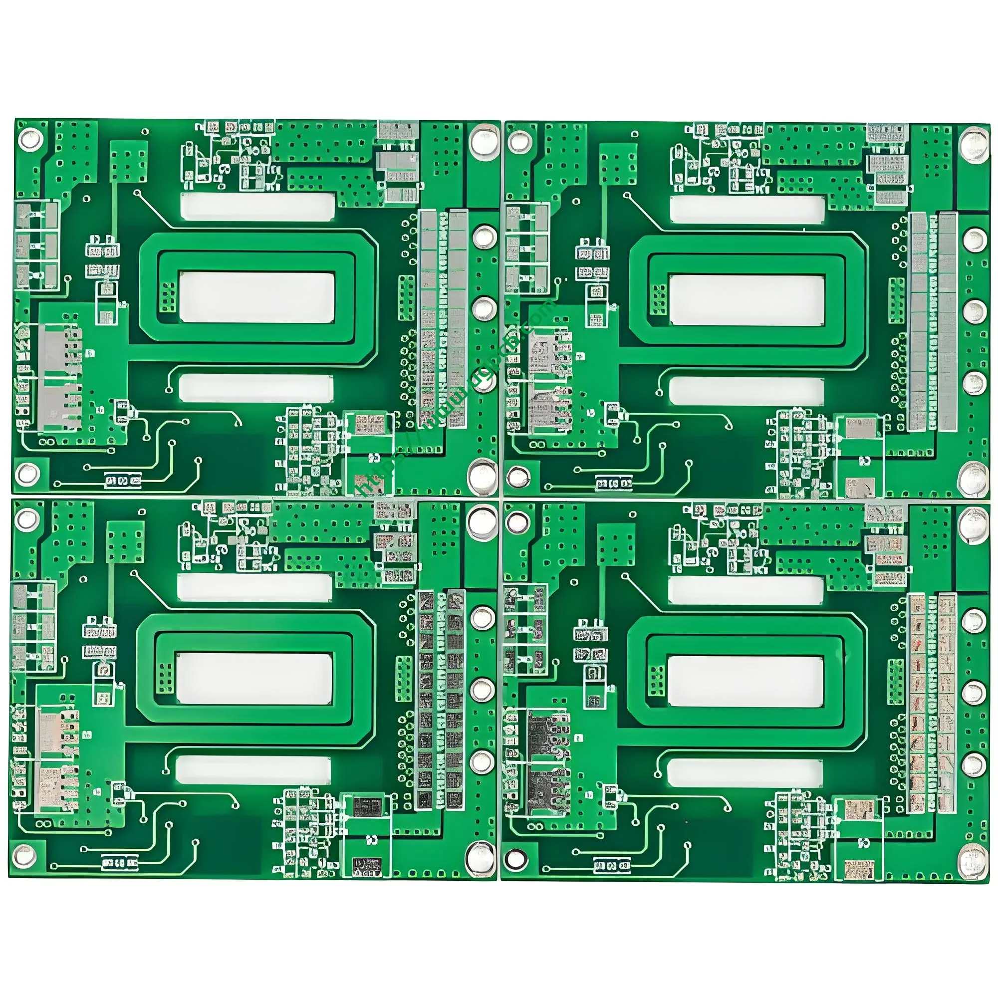
PCB สองด้านนิกเกิล-แพลเลเดียม-ทอง (หรือที่เรียกว่า PCB สองด้านของ ENEPIG) คือ แผงวงจรพิมพ์ ที่โดดเด่นด้วย Electroless Nickel Electroless Palladium Immersion Gold (เกี่ยวกับ enepic) พื้นผิวทั้งสองด้านของกระดาน. การรักษาพื้นผิวขั้นสูงนี้สร้างขึ้นจากโครงสร้าง PCB สองด้านแบบดั้งเดิมโดยการเพิ่มชั้นแพลเลเดียมระหว่างการสะสมของนิกเกิลและทองคำ, การสร้างพื้นผิวคอมโพสิตสามชั้นที่แข็งแกร่งซึ่งมีความสามารถในการบัดกรีที่เหนือกว่า, ประสิทธิภาพการยึดลวด, และความมั่นคงด้านสิ่งแวดล้อม.
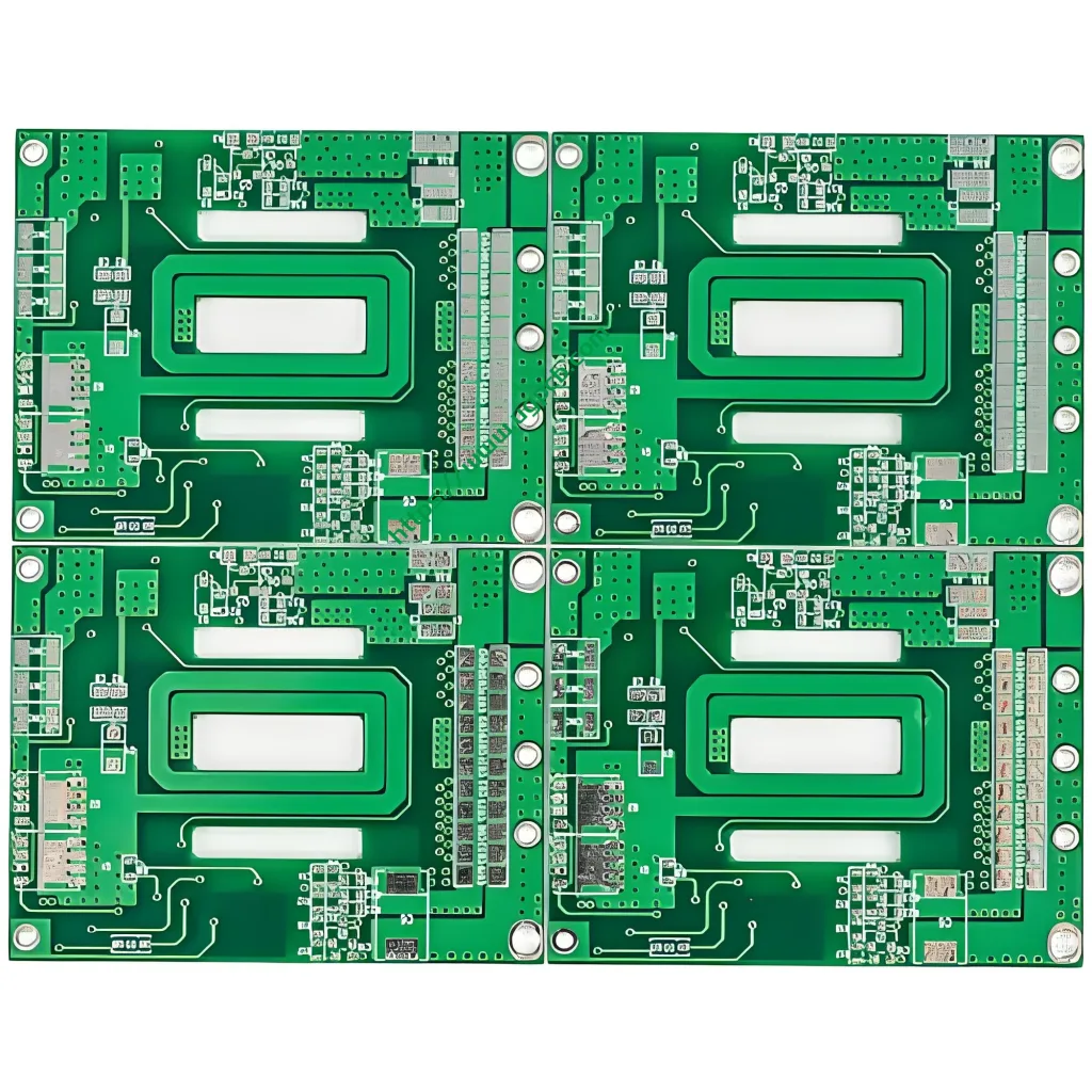
PCB สองด้านนิกเกิล - แพลเลเดียม - ทองของ UGPCB ใช้ลามิเนตหุ้มทองแดง Kingboard KB6160A FR-4 เป็นวัสดุฐาน. คณะกรรมการมีมาตรการ 49.6 × 32.8 มม. มีความหนา 1.6 มม. และความหนาของฟอยล์ทองแดง 1 ออนซ์ (ประมาณ 35 μm). หน้ากากประสานเป็นสีเขียวพร้อมตัวอักษรซิลค์สกรีนสีขาว. ด้วยค่ารูรับแสงต่ำสุดที่ 0.27 มม. และความกว้าง/ระยะห่างของเส้นขั้นต่ำ 0.27 × 0.3 มม, ENEPIG PCB นี้ให้การผลิตที่มีความแม่นยำผสมผสานกับการตกแต่งพื้นผิวคุณภาพสูง.
PCB นิกเกิล-แพลเลเดียม-ทองได้รับการยอมรับอย่างกว้างขวางว่าเป็น "การตกแต่งพื้นผิวแบบสากล" ในอุตสาหกรรมอิเล็กทรอนิกส์. มันรองรับการใช้งานที่หลากหลาย, รวมถึงโทรคมนาคม, อุปกรณ์อิเล็กทรอนิกส์สำหรับผู้บริโภค, การควบคุมอุตสาหกรรม, ระบบรักษาความปลอดภัย, อุปกรณ์อิเล็กทรอนิกส์ยานยนต์, แหล่งจ่ายไฟ, อุปกรณ์สมาร์ทโฮม, อุปกรณ์การแพทย์, และระบบการทหาร/การบินและอวกาศ.
ข้อกำหนดทางเทคนิคที่สำคัญ
| พารามิเตอร์ | ข้อมูลจำเพาะ |
|---|---|
| ลามิเนต | คิงบอร์ด KB6160A FR-4 |
| ความหนาของบอร์ด | 1.6 มม |
| จำนวนเลเยอร์ | สองด้าน |
| ขนาดกระดาน | 49.6 × 32.8 มม |
| รูรับแสงขั้นต่ำ | 0.27 มม |
| ความกว้าง/ระยะห่างบรรทัดขั้นต่ำ | 0.27 × 0.3 มม |
| ความหนาของฟอยล์ทองแดง | 1 ออนซ์ (➤35 ไมโครเมตร) |
| พื้นผิวเสร็จสิ้น | นิกเกิล-แพลเลเดียม-ทอง (เกี่ยวกับ enepic) |
| หน้ากากบัดกรี / ตำนาน | หน้ากากประสานสีเขียว / ซิลค์สกรีนสีขาว |
รายละเอียดลามิเนต: KB6160A FR-4 ลามิเนตเคลือบทองแดง
KB6160A เป็นลามิเนตหุ้มทองแดง FR-4 ประสิทธิภาพสูงที่ผลิตโดย Kingboard Laminates Holdings Ltd. วัสดุนี้ได้รับการออกแบบมาโดยเฉพาะสำหรับแผงสายไฟพิมพ์สองด้านมาตรฐาน (PWB) การผลิต. เป็นไปตามเอกสารข้อมูลจำเพาะ IPC-4101/21. คุณสมบัติที่สำคัญได้แก่:
- การปิดกั้น UV (ยูวีบี) ความสามารถ: ป้องกันการส่งผ่านแสงระหว่างการถ่ายภาพ, ปรับปรุงความแม่นยำและผลผลิตในการถ่ายโอนรูปแบบ
- ความเสถียรของมิติที่ดีเยี่ยม: รับประกันความเที่ยงตรงตลอดกระบวนการผลิต
- ทนความร้อนและคุณสมบัติทางกลที่เหนือกว่า: ตรงตามข้อกำหนดการใช้งานที่มีความน่าเชื่อถือสูง
- อุณหภูมิการเปลี่ยนแก้ว (ทีจี): 135องศาเซลเซียส (วิธีดีเอสซี)
- อุณหภูมิการสลายตัวทางความร้อน (TD): 305องศาเซลเซียส (วิธี TGA)
- Z-Axis CTE (เอ1/เอ2): 58 ppm/° C (< ทีจี) / 286 ppm/° C (> ทีจี)
- ค่าคงที่ไดอิเล็กตริก (ดีเค): 4.58
- ปัจจัยการกระจาย (ฟ): 0.022
- ความต้านทานระดับเสียง: 1 × 10⁸ MΩ-ซม
- การดูดซับความชื้น: 0.21%
- คะแนนความไวไฟ: UL94 วี-0
(ข้อมูลข้างต้นได้มาจากเอกสารข้อมูลทางเทคนิคของ Kingboard KB6160A, ด้วยวิธีการทดสอบตามมาตรฐานซีรีส์ IPC-TM-650)
พื้นผิวสำเร็จของ ENEPIG: คำอธิบายโดยละเอียด
เอเนพิกคืออะไร?
ENEPIG ย่อมาจาก Electroless Nickel Electroless Palladium Immersion Gold. เป็นการรักษาพื้นผิวโดยไม่ใช้สารเคมีโดยใช้ไฟฟ้าซึ่งจะสะสมชั้นโลหะสามชั้นตามลำดับ นั่นคือ นิกเกิล, แพลเลเดียม, และทอง—บนวงจรทองแดงของ พีซีบี.
โครงสร้างสามชั้นของ ENEPIG ประกอบด้วย:
- ชั้นล่าง – นิกเกิลแบบไม่ใช้ไฟฟ้า (ใน): ความหนา 3–5 μm. ชั้นนี้ทำหน้าที่เป็นเกราะป้องกันการแพร่กระจาย, ป้องกันการเคลื่อนตัวของทองแดงสู่พื้นผิวในขณะที่ให้การสนับสนุนทางกลและเป็นรากฐานสำหรับการบัดกรี.
- ชั้นกลาง – แพลเลเดียมแบบไม่ใช้ไฟฟ้า (ป.ล): ความหนา 0.05–0.1 ไมโครเมตร. ชั้นกั้นที่สำคัญนี้จะช่วยป้องกันปฏิสัมพันธ์ระหว่างนิกเกิลและทอง, ขจัดการกัดกร่อนของกัลวานิก.
- ชั้นบนสุด – ทองคำแช่ (AU): ความหนา 0.03–0.05 ไมโครเมตร. ชั้นบางนี้ให้ความสามารถในการบัดกรีและป้องกันการเกิดออกซิเดชันได้ดีเยี่ยม.
อ้างอิงจาก IPC-4556A (ล่าสุด 2025 การแก้ไข), ข้อกำหนดความหนาของชั้นเคลือบของ ENEPIG มีระบุไว้ดังต่อไปนี้:
- ชั้นนิกเกิล: 3 ไมโครเมตรถึง 6 μm (วัดที่ค่าเฉลี่ย ± 4σ)
- ชั้นแพลเลเดียม: 0.05 ไมโครเมตรถึง 0.30 μm (วัดที่ค่าเฉลี่ย ± 4σ)
- ชั้นทอง: ขั้นต่ำ 0.030 μm, สูงสุด 0.07 μm (วัดที่ต่ำกว่าค่าเฉลี่ย − 4σ)
(ข้อมูลจำเพาะด้านความหนาข้างต้นอ้างอิงจาก IPC-4556A, ข้อมูลจำเพาะสำหรับนิกเกิลแบบไม่ใช้ไฟฟ้า/แพลเลเดียมแบบไม่ใช้ไฟฟ้า/ทองแช่ (เกี่ยวกับ enepic) การชุบสำหรับบอร์ดพิมพ์)
ผังกระบวนการของ ENEPIG
PCB สองด้านนิกเกิล-แพลเลเดียม-ทองของ UGPCB เป็นไปตามกระบวนการชุบแบบไม่ใช้ไฟฟ้าที่ได้มาตรฐาน:
การล้างไขมัน → การแกะสลักแบบไมโคร → การจุ่มล่วงหน้า → การเปิดใช้งาน → การชุบนิกเกิลแบบไม่ใช้ไฟฟ้า → การชุบแพลเลเดียมแบบไม่ใช้ไฟฟ้า → การชุบทองแบบแช่ → การอบแห้ง
แต่ละขั้นตอนของกระบวนการประกอบด้วยขั้นตอนการล้างหลายขั้นตอนเพื่อให้มั่นใจในคุณภาพการชุบและการยึดเกาะ. ปฏิกิริยาเคมีที่เกี่ยวข้อง ได้แก่ ปฏิกิริยาออกซิเดชันรีดิวซ์และปฏิกิริยาการแทนที่.
ข้อได้เปรียบหลักของ PCB สองด้านนิกเกิล-แพลเลเดียม-ทอง
1. ขจัดข้อบกพร่อง “แผ่นดำ” อย่างสมบูรณ์
อีนิก (ทองคำแช่นิเกิลแบบไม่ใช้ไฟฟ้า) กระบวนการได้รับผลกระทบจากข้อบกพร่อง "แผ่นดำ" มานานแล้ว ซึ่งเป็นสภาวะที่การโจมตีด้วยทองบนชั้นนิกเกิลทำให้เกิดข้อต่อที่เปราะและความล้มเหลวก่อนวัยอันควร. ENEPIG แก้ปัญหานี้ด้วยการใช้ชั้นกั้นแพลเลเดียมระหว่างนิกเกิลและทอง, ป้องกันการสัมผัสโดยตรงและกำจัดการกัดกร่อนของขอบเกรน. ข้อมูลอุตสาหกรรมแสดงให้เห็นว่า ENEPIG ลดการเกิดแผ่นดำได้เกือบ 90% เมื่อเทียบกับ ENIG. ภายใต้สภาวะการปั่นจักรยานที่มีอุณหภูมิสูงมาก, ENEPIG สาธิตถึง 30% ความน่าเชื่อถือสูงกว่า ENIG.
2. ความสามารถในการยึดติดลวดที่เหนือกว่า
พื้นผิวสำเร็จของ ENEPIG ให้ประสิทธิภาพการยึดเกาะที่ดีเยี่ยมสำหรับทั้งลวดทองและอะลูมิเนียม. ชั้นแพลเลเดียมจะขยายหน้าต่างกระบวนการสำหรับการติดลวดทองให้กว้างขึ้น, ช่วยให้สามารถเชื่อมลวดได้อย่างน่าเชื่อถือแม้จะมีการสะสมของทองคำที่บางกว่าก็ตาม. ในการใช้งานมากมาย, ENEPIG รองรับความแข็งแรงในการติดลวดที่เกิน 10 กรัมสำหรับพันธะลวดทองและอลูมิเนียม. ทำให้ PCB สองด้านนิกเกิล-แพลเลเดียม-ทองเหมาะอย่างยิ่งสำหรับบรรจุภัณฑ์เซมิคอนดักเตอร์และการใช้งานประกอบแบบไฮบริดที่ต้องการการเชื่อมด้วยลวด.
3. ความสามารถในการบัดกรีที่ดีเยี่ยมและความทนทานต่อการไหลซ้ำหลายครั้ง
พื้นผิวสำเร็จของ ENEPIG ให้ความสามารถในการบัดกรีที่ดีเยี่ยมด้วยการบัดกรีทั้งแบบมีสารตะกั่วและไร้สารตะกั่ว (รวมถึงโลหะผสม SAC305). PCB สำเร็จรูปจาก ENEPIG สามารถทนทานได้ถึง 10 วงจรการรีโฟลว์โดยไม่มีการย่อยสลายอย่างมีนัยสำคัญ.
4. ขยายอายุการเก็บรักษา
ขอบคุณชั้นแพลเลเดียมป้องกัน, ผิวสำเร็จของ ENEPIG ให้ความต้านทานต่อการเกิดออกซิเดชันและการกัดกร่อนที่เหนือกว่า. ซึ่งส่งผลให้อายุการเก็บรักษายาวนานขึ้นอย่างมากเมื่อเทียบกับการตกแต่งพื้นผิวอื่นๆ. ตามแนวทาง IPC, พื้นผิวสำเร็จของ ENEPIG สามารถอยู่ในประเภท IPC 3 อายุการเก็บรักษาอย่างน้อยสิบสองเดือน.
5. ความยืดหยุ่นในการออกแบบที่มากขึ้น
ต่างจากกระบวนการอิเล็กโทรไลต์นิกเกิล-ทอง, ENEPIG เป็นกระบวนการไม่ใช้ไฟฟ้าที่ไม่ต้องใช้บัสบาร์หรือสายชุบ. ช่วยให้สามารถประมวลผลบอร์ดได้มากขึ้นพร้อมกันในอ่างชุบเดียวกัน, เพิ่มปริมาณงานโดยรวม. นอกจากนี้, ENEPIG ไม่มีข้อจำกัดด้านเส้นทาง, ให้ความยืดหยุ่นมากขึ้นสำหรับการออกแบบวงจรความหนาแน่นสูง.
PCB สองด้านนิกเกิล-แพลเลเดียม-ทองทำงานอย่างไร
การทำงานร่วมกันของการชุบสามชั้น
ประสิทธิภาพที่โดดเด่นของ PCB สองด้านนิกเกิล-แพลเลเดียม-ทองเกิดจากการประสานกันที่แม่นยำของชั้นชุบทั้งสามชั้น:
① ชั้นนิกเกิล (โลหะผสม Ni-P) – อุปสรรคของมูลนิธิ
ชั้นนิกเกิลทำหน้าที่เป็นรากฐานของโครงสร้าง ENEPIG. หน้าที่หลักของมันคือป้องกันการแพร่กระจายของอะตอมของทองแดงสู่พื้นผิว, ป้องกันการก่อตัวของสารประกอบระหว่างโลหะ Cu-Sn ที่เปราะ (ไอเอ็มซี) ระหว่างการบัดกรีหรือการสัมผัสที่อุณหภูมิสูง. โดยทั่วไปความหนาของนิกเกิลจะถูกควบคุมระหว่าง 3–6 μm, โดยมีปริมาณฟอสฟอรัสคงอยู่อย่างเคร่งครัดที่ 7-9% เพื่อความสมดุลของความแข็งและความต้านทานการกัดกร่อน.
② ชั้นแพลเลเดียม (ป.ล) – Critical Barrier และเลเยอร์การเปิดใช้งาน
ชั้นแพลเลเดียมเป็นคุณสมบัติที่กำหนดความแตกต่างระหว่าง ENEPIG และ ENIG. ทำหน้าที่เป็น “ผนังกั้นห้อง”,” ป้องกันการโยกย้ายและการกัดกร่อนขอบเกรนระหว่างนิกเกิลและทอง. ชั้นแพลเลเดียมจะต้องมีความหนาพอที่จะป้องกันการแพร่กระจายของนิกเกิลไปยังพื้นผิวทอง และป้องกันการกัดกร่อนที่มากเกินไปของการสะสมของนิกเกิลแบบไม่ใช้ไฟฟ้า.
3 ชั้นทองคำ (AU) - การป้องกันและการบัดกรี
ชั้นทองด้านนอกบาง ๆ ช่วยปกป้องนิกเกิลจากการเกิดออกซิเดชัน ในขณะเดียวกันก็ให้ความต้านทานต่อการสัมผัสต่ำและความสามารถในการบัดกรีที่ดีเยี่ยม. เพราะชั้นแพลเลเดียมให้การแยกตัว, ชั้นทองใน ENEPIG สามารถทำให้บางลงได้ (0.03–0.05 ไมโครเมตร) โดยไม่กระทบต่อความน่าเชื่อถือ, ซึ่งช่วยลดต้นทุนวัสดุได้ในระดับหนึ่ง.
การจำแนกประเภทของ PCB สองด้านนิกเกิล-แพลเลเดียม-ทอง
PCB สองด้านนิกเกิล-แพลเลเดียม-ทองของ UGPCB สามารถจำแนกทางวิทยาศาสตร์ได้ในหลายมิติ:
ตามจำนวนเลเยอร์
- PCB สองด้าน: วงจรนำไฟฟ้าจะกระจายอยู่ทั้งสองด้านของวัสดุพิมพ์, ด้วยการเชื่อมต่อไฟฟ้าที่สร้างผ่านรูทะลุที่ชุบ (บ่น).
โดยวัสดุฐาน
- FR-4 ลามิเนตผ้าแก้วอีพ็อกซี่: ใช้ Kingboard KB6160A, สอดคล้องกับ IPC-4101/21.
โดยพื้นผิวเสร็จสิ้น
- เกี่ยวกับ enepic (อิเล็กโทรไลต์นิกเกิลอิเล็กโทรไลเซิลแพลเลเดียม) : โครงสร้างการชุบคอมโพสิตสามชั้น.
ตามโดเมนแอปพลิเคชัน
- PCB วัตถุประสงค์ทั่วไปที่มีความน่าเชื่อถือสูง: เหมาะสำหรับงานโทรคมนาคม, อุปกรณ์อิเล็กทรอนิกส์ยานยนต์, อุปกรณ์การแพทย์, การบินและอวกาศ, การควบคุมอุตสาหกรรม, และอีกมาก.
โดยการผลิตที่มีความแม่นยำ
- PCB ที่มีความแม่นยำ: รูรับแสงขั้นต่ำของ 0.27 มม, ความกว้างบรรทัดขั้นต่ำ / ระยะห่างของ 0.27 × 0.3 มม.
ผังกระบวนการผลิต
การผลิต PCB สองด้านนิกเกิล-แพลเลเดียม-ทองของ UGPCB เป็นไปตามขั้นตอนการผลิตที่ครอบคลุม:
เวที 1: การเตรียมพื้นผิว
- การตัดวัสดุ: ลามิเนตหุ้มทองแดง KB6160A ถูกตัดตามขนาดที่ต้องการ.
- การขุดเจาะ: การเจาะด้วยกลไกด้วยรูรับแสงขั้นต่ำ 0.27 มม.
- การสะสมทองแดงแบบไม่ใช้ไฟฟ้า & การชุบแผง: การทำให้เป็นโลหะผ่านรู.
เวที 2: การก่อตัวของวงจร
- การถ่ายโอนรูปแบบ: การเคลือบฟิล์มแห้ง → การเปิดรับแสง → การพัฒนา.
- การแกะสลักวงจร: การนำทองแดงส่วนเกินออกเพื่อสร้างรูปแบบวงจร.
- Aoi (การตรวจสอบด้วยแสงอัตโนมัติ) : รับประกันความถูกต้องของวงจร.
เวที 3: หน้ากากประสานและตำนาน
- การพิมพ์หน้ากากประสาน: การใช้หมึกสีเขียวเพื่อป้องกันวงจรและป้องกันการบัดกรี.
- การพิมพ์ในตำนาน: ตัวอักษรซิลค์สกรีนสีขาว.
เวที 4: พื้นผิวเสร็จสิ้น (เกี่ยวกับ enepic)
- การล้างไขมัน: การกำจัดสิ่งปนเปื้อนบนพื้นผิว.
- การแกะสลักแบบไมโคร: การแกะสลักพื้นผิวทองแดงเล็กน้อยเพื่อเพิ่มการยึดเกาะ.
- ก่อนจุ่ม: การปรับสภาพก่อนเปิดใช้งาน.
- การเปิดใช้งาน: การสะสมของชั้นเมล็ดแพลเลเดียมเร่งปฏิกิริยาบนทองแดง.
- การชุบนิเกิลแบบไม่ใช้ไฟฟ้า: การสะสมของชั้นนิกเกิล (3–5 ไมโครเมตร).
- การชุบแพลเลเดียมแบบไม่ใช้ไฟฟ้า: การสะสมของชั้นแพลเลเดียม (0.05–0.1 ไมโครเมตร).
- การชุบทองแช่: การสะสมของชั้นทองคำ (0.03–0.05 ไมโครเมตร).
- การอบแห้ง: เสร็จสิ้นการตกแต่งพื้นผิว.
เวที 5: การตรวจสอบขั้นสุดท้าย
- การทดสอบไฟฟ้า: รับประกันความต่อเนื่องและการแยกทางไฟฟ้า.
- การตรวจสอบภาพ: การตรวจสอบคุณภาพพื้นผิว.
- การบรรจุหีบห่อ & การส่งสินค้า.
การใช้งานทั่วไป
PCB สองด้านนิกเกิล-แพลเลเดียม-ทองของ UGPCB ถูกนำมาใช้กันอย่างแพร่หลายในอุตสาหกรรมต่างๆ มากมาย:
อุปกรณ์โทรคมนาคม
- สถานีฐาน, เราเตอร์, สวิตช์
- โมดูลการสื่อสารความถี่สูง, อุปกรณ์คลื่นความถี่วิทยุ
อุปกรณ์อิเล็กทรอนิกส์ยานยนต์
- หน่วยควบคุมเครื่องยนต์ (กล่อง ECU)
- ระบบสาระบันเทิงภายในรถยนต์
- อดาส (ระบบช่วยเหลือผู้ขับขี่ขั้นสูง)
- BMS (ระบบการจัดการแบตเตอรี่) สำหรับยานยนต์พลังงานใหม่

อุปกรณ์การแพทย์
- อุปกรณ์ฝังทางการแพทย์
- เครื่องมือวินิจฉัย, อุปกรณ์ติดตามผู้ป่วย
การบินและอวกาศ & การป้องกัน
- ยานอวกาศและอุปกรณ์อิเล็กทรอนิกส์ดาวเทียม
- ระบบควบคุมการบิน
การควบคุมอุตสาหกรรม & ความปลอดภัย
- PLC (คอนโทรลเลอร์ลอจิกที่ตั้งโปรแกรมได้)
- มอเตอร์ขับเคลื่อนอุตสาหกรรม
- อุปกรณ์รักษาความปลอดภัยและการเฝ้าระวัง
อุปกรณ์อิเล็กทรอนิกส์สำหรับผู้บริโภค & บ้านอัจฉริยะ
- เมนบอร์ดสมาร์ทโฟน
- โมดูลควบคุมบ้านอัจฉริยะ
- อุปกรณ์สวมใส่ได้
ทหาร & เพาเวอร์อิเล็กทรอนิกส์
- ระบบอิเล็กทรอนิกส์ทางการทหาร
- โมดูลพลังงาน, ตัวแปลงไฟ
เหตุใดจึงเลือก UGPCB สำหรับ PCB สองด้านนิกเกิล-แพลเลเดียม-ทอง?
✅ การปฏิบัติตามมาตรฐาน IPC
PCB สองด้านนิกเกิล - แพลเลเดียม - ทองของ UGPCB ผลิตขึ้นตามมาตรฐาน IPC-4556A อย่างเคร่งครัด. ลามิเนต KB6160A เป็นไปตามมาตรฐาน IPC-4101/21, ทำให้มั่นใจได้ถึงมาตรฐานเต็มรูปแบบตั้งแต่วัสดุฐานไปจนถึงการตกแต่งพื้นผิว.
✅ความสามารถในการผลิตที่แม่นยำ
ด้วยค่ารูรับแสงต่ำสุดที่ 0.27 มม. และความกว้าง/ระยะห่างบรรทัดขั้นต่ำของ 0.27 × 0.3 มม, UGPCB ตอบสนองความต้องการของการเชื่อมต่อระหว่างกันที่มีความหนาแน่นสูง (HDI) และการประกอบชิ้นส่วนที่มีระยะพิทช์ละเอียด.
✅ รับประกันความน่าเชื่อถือสูง
พื้นผิวของ ENEPIG ช่วยลดข้อบกพร่องของแผ่นดำได้เกือบหมด 90% และจัดส่งได้ถึง 30% ความน่าเชื่อถือสูงกว่า ENIG ภายใต้ความผันผวนของอุณหภูมิที่รุนแรง. ผลิตภัณฑ์ทนทานต่อรอบการรีโฟลว์หลายรอบและตรงตามมาตรฐาน J-STD-003 หมวดหมู่ 3 ข้อกำหนดด้านความทนทาน.
✅ การสนับสนุนด้านเทคนิคอย่างมืออาชีพ
ทีมงาน UGPCB ให้การสนับสนุนด้านเทคนิคอย่างเต็มรูปแบบ, ตั้งแต่การตรวจสอบไฟล์ Gerber และการเพิ่มประสิทธิภาพ BOM ไปจนถึงการประกอบ PCBA.
สอบถามรายละเอียดเพิ่มเติม & การสั่งซื้อ
พร้อมที่จะเปลี่ยนการออกแบบของคุณให้เป็น PCB สองด้านนิกเกิล-แพลเลเดียม-ทองคุณภาพสูง?
📧 อีเมล: sales@ugpcb.com
📞 โทรศัพท์: +86-135 4412 8719
🌐 เว็บไซต์: www.ugpcb.com
📋 ขั้นตอนการสั่งซื้อ:
- ส่งไฟล์ Gerber, ระเบิด, และเอกสารการออกแบบ.
- ทีมวิศวกรของ UGPCB ดำเนินการ DFM (ออกแบบเพื่อการผลิต) ทบทวน.
- การยืนยันคำสั่งซื้อและกำหนดการส่งมอบ.
- การผลิตและการควบคุมคุณภาพ.
- การติดตามการจัดส่งและลอจิสติกส์.
ไม่ว่าคุณจะต้องการ PCB Prototyping หรือปริมาณการผลิต, UGPCB มุ่งมั่นที่จะนำเสนอ PCB สองด้านนิกเกิล-แพลเลเดียม-ทองคุณภาพสูง และบริการด้านเทคนิคระดับมืออาชีพ.
การประกาศแหล่งข้อมูล
ข้อมูลทางเทคนิคและข้อกำหนดมาตรฐานที่อ้างถึงในเอกสารนี้ได้มาจากองค์กรที่เชื่อถือได้ดังต่อไปนี้:
- ไอพีซี-4556A: ข้อมูลจำเพาะสำหรับนิกเกิลแบบไม่ใช้ไฟฟ้า/แพลเลเดียมแบบไม่ใช้ไฟฟ้า/ทองแช่ (เกี่ยวกับ enepic) การชุบสำหรับบอร์ดพิมพ์ (2025 การแก้ไข)
- IPC-4101/21: ข้อกำหนดสำหรับวัสดุฐานสำหรับบอร์ดพิมพ์แข็งและหลายชั้น – เอกสารข้อมูลจำเพาะที่ใช้กับ KB6160A
- เอกสารข้อมูลทางเทคนิค Kingboard KB6160A (คิงบอร์ด ลามิเนทส์ โฮลดิ้งส์ จำกัด)
- IPC-TM-650: คู่มือวิธีทดสอบ – วิธีทดสอบมาตรฐานที่ใช้สำหรับการวัดคุณสมบัติของวัสดุ
- เจ-STD-003: การทดสอบความสามารถในการบัดกรีสำหรับบอร์ดพิมพ์ – มาตรฐานการทดสอบความสามารถในการบัดกรี
- UL94: มาตรฐานการทดสอบความไวไฟของวัสดุพลาสติกสำหรับชิ้นส่วนในอุปกรณ์และเครื่องใช้ – มาตรฐานการติดไฟ
ข้อมูลทั้งหมดที่อ้างถึงข้างต้นมาจากมาตรฐานอย่างเป็นทางการและเอกสารทางเทคนิคที่ระบุไว้, รับประกันความถูกต้องและอำนาจ.













