|ในยุคของการส่งข้อมูลแบบมัลติกิกะบิต, ค่าเบี่ยงเบนอิมพีแดนซ์ระดับไมครอนบน PCB อาจทำให้ประสิทธิภาพของอาร์เรย์เซิร์ฟเวอร์ที่มีมูลค่านับล้านลดลง.
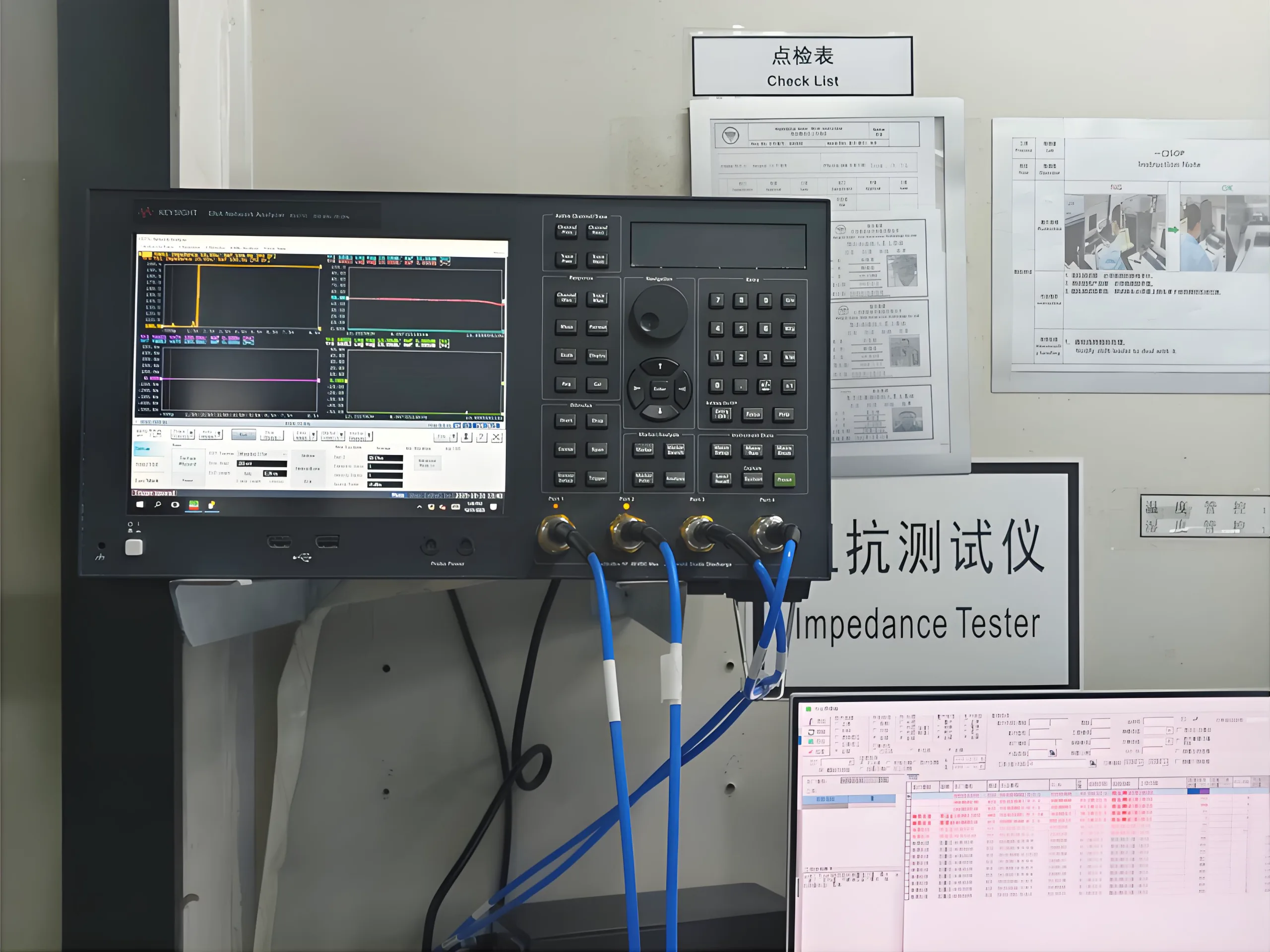
ที่สถานที่ของ UGPCB, วิศวกรตรวจสอบข้อมูลอิมพีแดนซ์สำหรับมาเธอร์บอร์ดเซิร์ฟเวอร์ความเร็วสูงแบบเรียลไทม์. ส่วนโค้งบนหน้าจอจะคงอยู่ภายใน แถบผ่านสีเขียว100Ω ± 2% — ที่ ข้อกำหนดที่เข้มงวดของ PCIe 5.0 มาตรฐานสำหรับอิมพีแดนซ์ดิฟเฟอเรนเชียล. สิ่งนี้เกิดขึ้นได้ด้วยการลงทุนครั้งล่าสุดของเราในด้านความล้ำหน้า พีซีบี การทดสอบและ การควบคุมคุณภาพ เทคโนโลยี.
ความท้าทายด้านอุตสาหกรรม: วิกฤตการณ์ที่แม่นยำในยุคสัญญาณความเร็วสูง
การเติบโตอย่างรวดเร็วของการประมวลผล AI และการสื่อสาร 5G ทำให้เกิดความต้องการอัตราข้อมูลที่เร็วขึ้นแบบทวีคูณ. มาตรฐานเช่น PCIe ได้พัฒนาไป PCIE 5.0/6.0, ที่มีความถี่สัญญาณเกิน 32 GT/s และมุ่งหน้าไปยัง 64 GT/วินาที.
ความถี่ที่สูงขึ้นทำให้การสูญเสียการแทรกเพิ่มขึ้นแบบทวีคูณ, ในขณะที่อิมพีแดนซ์ไม่ต่อเนื่องใน ร่องรอย PCB ทำให้เกิดสัญญาณสะท้อนและความกระวนกระวายใจ. ปัญหาเหล่านี้แสดงถึงความท้าทายด้านความสมบูรณ์ของสัญญาณที่สำคัญที่สุด การออกแบบ PCB ความเร็วสูง และการผลิต.
เมนบอร์ดสมาร์ทโฟนสมัยใหม่อาจมีอย่างน้อย 12 ชั้น ของเส้นทางที่ซับซ้อน. แนวโน้มของการย่อขนาดอย่างไม่หยุดยั้งต้องการความกว้างของรอยเส้นที่แคบลงและระยะห่างที่แคบลง, ผลักดันข้อกำหนดสำหรับ การควบคุมความต้านทาน ในการผลิต PCB สู่ระดับที่ไม่เคยมีมาก่อน.
โซลูชันทางเทคนิค: ระบบทดสอบความต้านทาน Keysight ของ UGPCB
เพื่อจัดการกับความท้าทายเหล่านี้, UGPCB ได้บูรณาการ ระบบทดสอบความต้านทาน Keysight 4-Channel 20G, แพลตฟอร์มที่มีความแม่นยำสูงซึ่งใช้ Vector Network Analyzer (VNA) เทคโนโลยี.
การใช้ประโยชน์หลักของระบบ เทคโนโลยีวิเคราะห์เครือข่ายประสิทธิภาพสูงของ Keysight, เนื้อเรื่อง 4 ช่องทดสอบอิสระ โดยมีช่วงความถี่ตั้งแต่ 10 เมกะเฮิรตซ์ถึง 20 กิกะเฮิรตซ์. ย่านความถี่กว้างนี้ช่วยให้สามารถประเมินการเชื่อมต่อระหว่างกันความเร็วสูงได้อย่างครอบคลุม, ตั้งแต่วงจรดิจิทัลพื้นฐานไปจนถึงการใช้งานคลื่นมิลลิเมตร.
ข้อดีของระบบ: สามแห่งความแม่นยำ, ประสิทธิภาพ, และความมั่นคง
-
ความแม่นยำที่ไม่มีใครเทียบได้: ระบบให้ความแม่นยำในการวัดอิมพีแดนซ์พื้นฐานที่ ±0.08% (โดยทั่วไป ± 0.045%), โดยมีช่วงอิมพีแดนซ์ตั้งแต่ 25 mΩถึง 40 MΩ. ระดับนี้ การทดสอบความต้านทานของ PCB ความแม่นยำในการตรวจจับความเบี่ยงเบนที่นาทีที่สุด, ซึ่งเป็นสิ่งสำคัญสำหรับ การผลิต PCBA ขั้นสูง.
-
ประสิทธิภาพที่เหนือกว่า: มันรองรับ การทดสอบแบบขนานหลายช่องสัญญาณ, ปรับปรุงปริมาณงานได้ถึง 300% เมื่อเทียบกับอุปกรณ์ช่องเดียว. ช่วยให้สามารถวางแผนการทดสอบอัตโนมัติได้ 24/7 ความสามารถในการทดสอบแบทช์, เพรียวลม ต้นแบบ PCB และการชุมนุม กระบวนการตรวจสอบ.
-
เสถียรภาพที่ยอดเยี่ยม: นำเสนอ เทคโนโลยีการชดเชยอุณหภูมิ และระบบแสงที่สร้างขึ้นด้วยวัสดุที่มีการขยายตัวต่ำ, ระบบจะลดผลกระทบจากความแปรผันของสภาพแวดล้อมที่มีต่อผลการวัดให้เหลือน้อยที่สุด, รับรองข้อมูลที่สอดคล้องกันเพื่อความน่าเชื่อถือ การประกันคุณภาพ PCB.
แอปพลิเคชัน & ค่า: คุณภาพครบวงจรตั้งแต่ต้นแบบจนถึงการผลิต
ระบบขั้นสูงนี้มอบคุณค่าทั่วทั้งขอบเขตการบริการของ UGPCB, ตอกย้ำความเป็นผู้นำของเราในด้าน PCB มืออาชีพและ การผลิต PCBA บริการ.
-
ในร&D และการสร้างต้นแบบ: วิศวกรสามารถตรวจสอบได้อย่างรวดเร็วว่าสแต็คอัพและวัสดุที่แตกต่างกันส่งผลต่ออิมพีแดนซ์อย่างไร, ลดรอบการทดสอบการออกแบบจากสัปดาห์เหลือเป็นวัน. สิ่งนี้จะช่วยเร่งการพัฒนาของ PCB ความถี่สูง, RF PCB, และ HDI PCBS.
-
ในการควบคุมคุณภาพการผลิตจำนวนมาก: บูรณาการเข้ากับสายการผลิตอัจฉริยะ, ระบบจะสุ่มตัวอย่างหรือตรวจสอบทั้งหมด, การสร้างแผนภูมิ SPC แบบเรียลไทม์. ซึ่งช่วยให้สามารถปรับกระบวนการเชิงรุกได้, การป้องกันปัญหาแบทช์และรับประกันคุณภาพที่สม่ำเสมอ การผลิต PCB ในปริมาณมาก.
-
สำหรับการใช้งานระดับไฮเอนด์: สำหรับการใช้งานที่สำคัญเช่น PCB เซิร์ฟเวอร์ AI, 5สถานีฐานจี แผงวงจร, และสวิตช์ความเร็วสูง, UGPCB ให้รายละเอียด รายงานความสอดคล้องของอิมพีแดนซ์. ความโปร่งใสของข้อมูลนี้สร้างความไว้วางใจให้กับลูกค้าที่กำลังมองหา ซัพพลายเออร์ PCB ที่เชื่อถือได้ และ โซลูชั่น PCBA แบบครบวงจร.
วิทยาศาสตร์เบื้องหลังการวัดผล
ประสิทธิภาพของระบบมีรากฐานมาจากหลักการทางวิทยาศาสตร์ที่แข็งแกร่ง. มันจ้าง การสะท้อนกลับโดเมนเวลา (TDR), ซึ่งทำงานเหมือนกับเรดาร์โดยการส่งสัญญาณไปตามร่องรอยและวิเคราะห์การสะท้อนเพื่อระบุการเปลี่ยนแปลงอิมพีแดนซ์และข้อบกพร่อง.
ความต้านทานลักษณะเฉพาะ (Z₀) ของร่องรอยถูกกำหนดโดยเรขาคณิตเป็นหลัก และประมาณที่ความถี่สูงโดยสูตร:
ซี₀ data √(l/c)
(โดยที่ L คือการเหนี่ยวนำต่อความยาวหน่วย และ C คือความจุต่อความยาวหน่วย). สิ่งนี้เน้นย้ำว่าเหตุใดการควบคุมขนาดทางกายภาพจึงเป็นสิ่งสำคัญยิ่ง ควบคุมการผลิต PCB อิมพีแดนซ์.
ระบบยังใช้ วิธีเดลต้า-แอล, อัลกอริธึมขั้นสูงที่ยกเลิกเอฟเฟกต์ฟิกซ์เจอร์และลบการสะท้อนหลายครั้ง, มอบความแม่นยำที่เหนือกว่าสำหรับ การทดสอบ PCB ความเร็วสูงและความถี่สูง.
ผลประโยชน์ของลูกค้าที่จับต้องได้
การลงทุนในความสามารถนี้แปลเป็นข้อได้เปรียบของลูกค้าโดยตรง:
-
ความเสี่ยงลดลง: การตรวจจับความเบี่ยงเบนของอิมพีแดนซ์ตั้งแต่เนิ่นๆ จะช่วยป้องกันความล้มเหลวและการเรียกคืนภาคสนามซึ่งมีค่าใช้จ่ายสูง.
-
ประสิทธิภาพที่เพิ่มขึ้น: การควบคุมอิมพีแดนซ์ที่แม่นยำช่วยให้อัตราข้อมูลสูงขึ้นและลดอัตราข้อผิดพลาดบิตลง, ซึ่งเป็นสิ่งสำคัญสำหรับ PCBA ดิจิตอลความเร็วสูง และ PCB ของอุปกรณ์สื่อสาร.
-
เวลาออกสู่ตลาดเร็วขึ้น: ข้อมูลการทดสอบที่เชื่อถือได้ช่วยลดความไม่แน่นอนในการออกแบบ, ลดเวลาการตรวจสอบสำหรับอินเทอร์เฟซความเร็วสูงโดย 40-60%.
ถึง UGPCB, ความมุ่งมั่นของเราไม่เพียงฝังอยู่บนผนังโรงงานของเราเท่านั้น แต่ยังฝังอยู่ในบอร์ดทุกแผ่นที่เราจัดส่งอีกด้วย: “ความต้านทานปลายเดี่ยว 50Ω ± 5%, อิมพีแดนซ์ดิฟเฟอเรนเชียล 100Ω ±8% — 30% เหนือกว่ามาตรฐานอุตสาหกรรมทั่วไป” นี่ไม่ใช่แค่ข้อกำหนดเท่านั้น; เป็นคำมั่นสัญญาของเราที่จะรักษาความสมบูรณ์ของสัญญาณในยุคดิจิทัลความเร็วสูง. โดยเลือก UGPCB สำหรับคุณ การผลิต PCB และชุดประกอบ PCBA ความต้องการ, คุณเป็นพันธมิตรกับผู้ผลิตที่มีอุปกรณ์ครบครันเพื่อมอบความแม่นยำในการออกแบบที่เป็นที่ต้องการมากที่สุดของคุณต้องการ.


