
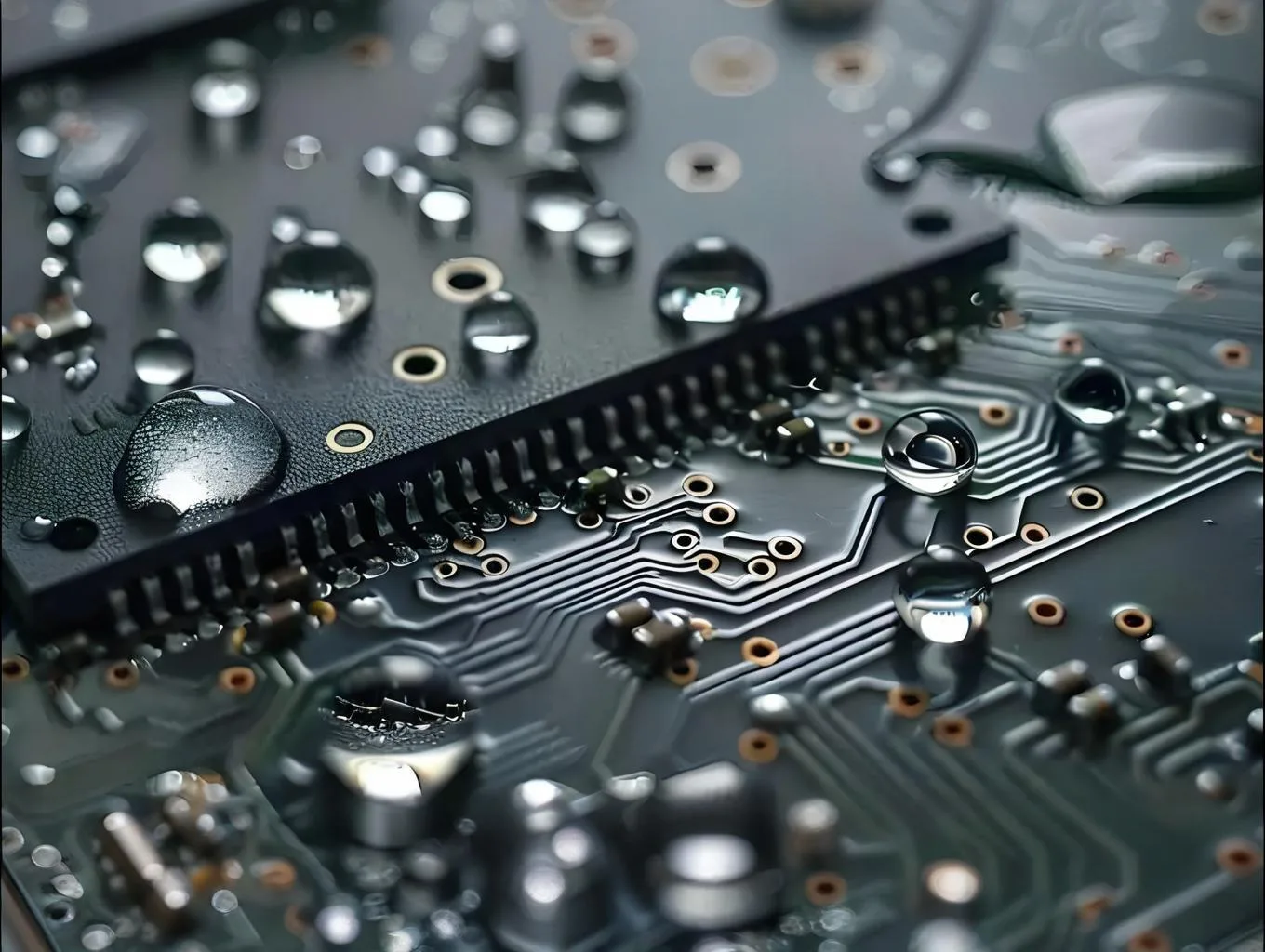
As electronic devices become increasingly sophisticated, a cutting-edge protective technology derived from aerospace applications is now safeguarding the reliability of every لوحة الدائرة.
This innovation is Plasma Nano-Coating, also known as ترسيب البخار الكيميائي المعزز بالبلازما (بيكفد). The nano-coating is a functional, مرن, and nanoscale-thin film characterized by its hydrophobic and oleophobic properties. Utilizing بيكفد تكنولوجيا, reactive gases are activated by plasma within a low-temperature vacuum chamber, initiating chemical reactions on the substrate surface to form a mesh-like protective film with nanoscale thickness.
This technology not only provides exceptional moisture, ماء, and corrosion resistance for bare مركبات ثنائي الفينيل متعدد الكلور and assembled PCBA circuit boards but also overcomes numerous limitations associated with traditional protection methods.
Technical Principle Analysis
طلاء البلازما نانو (بيكفد) technology represents an advanced approach to circuit board protection. It employs plasma to activate reactive gases in a low-temperature, low-pressure environment, forming a highly cross-linked nanoscale protective film.

The core of PECVD technology lies in decomposing reactive gases into active radicals via plasma. These radicals undergo chemical reactions on the substrate surface, resulting in an ultra-thin, uniform polymer coating.
The process temperature is typically low, avoiding potential thermal damage to electronic components and making it particularly suitable for fully assembled ثنائي الفينيل متعدد الكلور circuit boards.
Compared to traditional protective technologies, PECVD enables precise control over coating thickness at the nanoscale—for example, ranging from 15nm to 3000nm—achieving true microscopic protection.
PCB Protection Applications
In bare PCB protection, plasma nano-coating demonstrates unique value. Due to its extreme thinness, the coating has minimal impact on impedance matching and signal integrity, ensuring no interference with high-frequency circuit performance.
ل ربط عالية الكثافة (مؤشر التنمية البشرية) لوحات, PECVD technology can cover extremely fine line widths and spacing, addressing challenges that traditional protective materials fail to reliably protect.
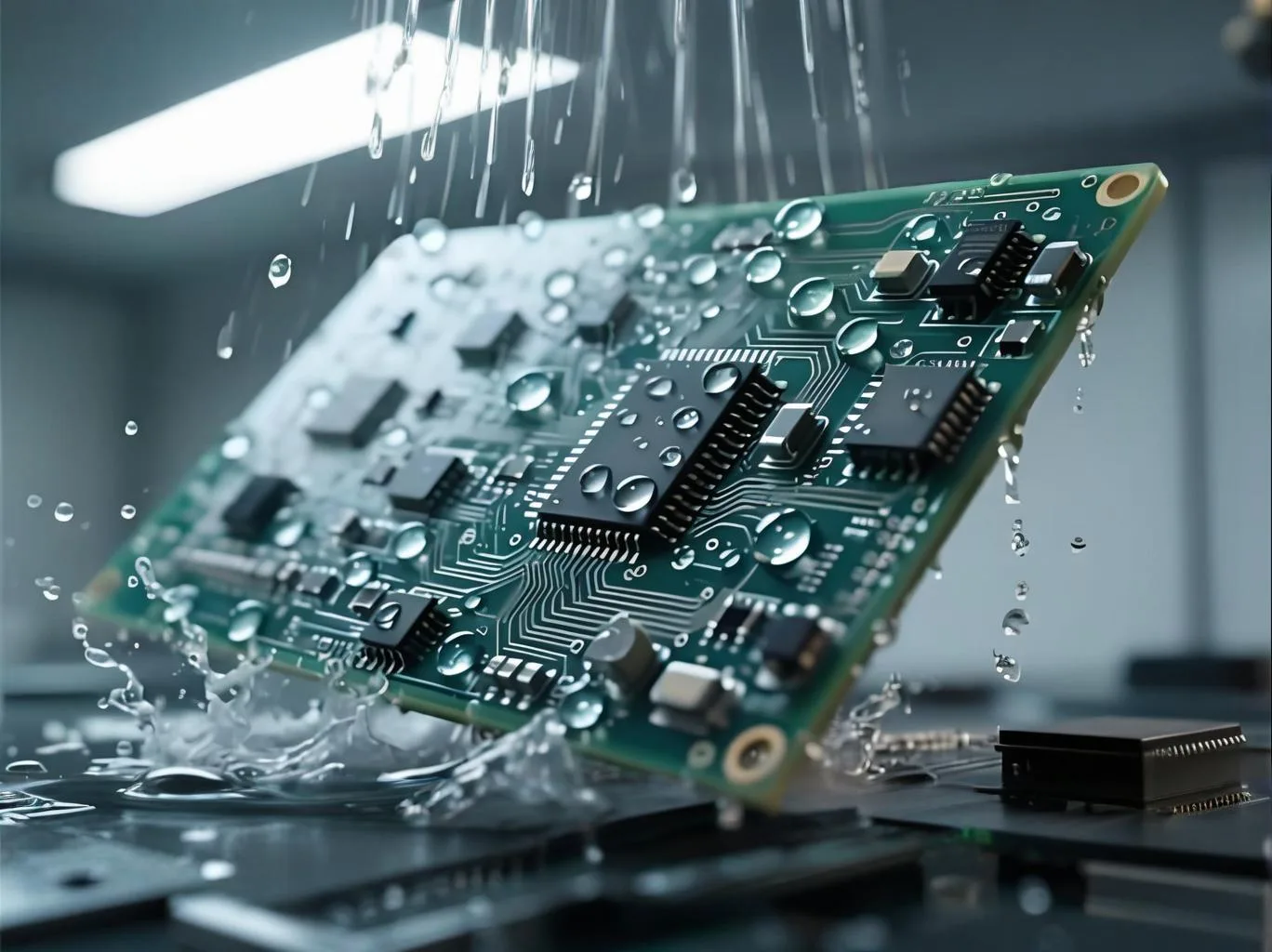
With a coating thickness of 15–40nm, an IPX1–2 splash resistance rating can be achieved. Increasing the thickness to 300–2500nm enables IPX4–8 immersion protection ratings.
This means that even electronic devices submerged in water for extended periods can have their core circuits reliably safeguarded.
PCBA Protection Solutions
For assembled PCBA circuit boards, plasma nano-coating technology excels in comprehensive coverage. As a gas-phase deposition process, the coating uniformly covers every corner of the PCBA, including areas under components, fine-pitch leads, and micro-gaps.
UGPCB’s plasma nano-protection technology is a leader in this field, offering the industry’s thinnest and reworkable conformal coating. This allows manufacturers to reduce scrap rates and improve production yields.
Unlike traditional conformal coatings, plasma nano-coating does not form excessively thick layers, eliminating the need for extensive connector masking. This significantly streamlines the production process and reduces manufacturing costs.
Research indicates that PCBA units with plasma nano-coating can reduce field failure repair rates by 40–60%, greatly enhancing product reliability and lowering after-sales costs.
Comparison with Traditional Protection Technologies
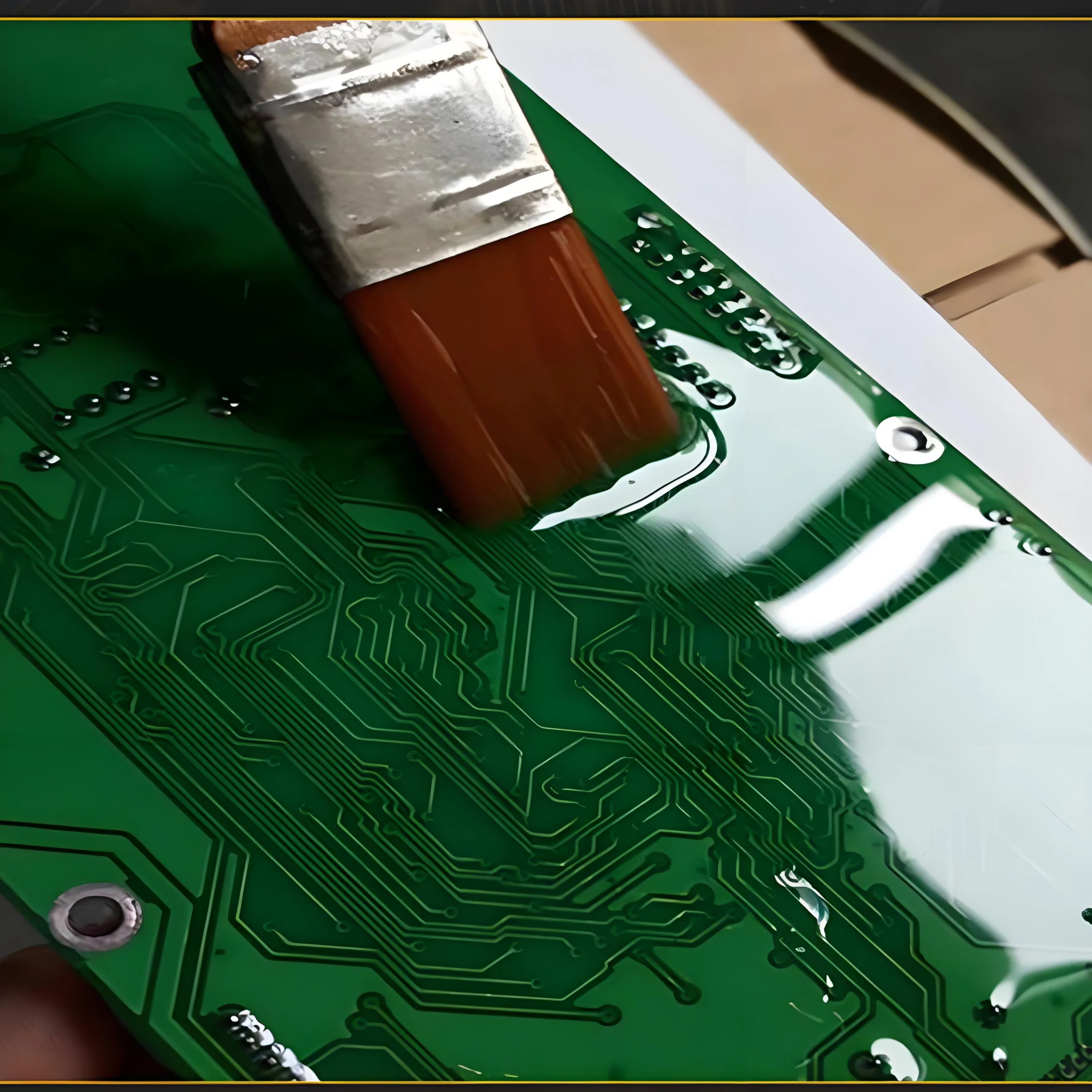
Traditional PCB protection methods have several limitations. Liquid-based conformal coatings are prone to uneven application, bubbling, and incomplete coverage in hidden areas. They also require heat curing, which emits significant amounts of carcinogenic VOC fumes.
While parylene (poly-p-xylylene) coatings offer excellent performance, they require high-vacuum, high-temperature processing environments, have low deposition rates, are non-reworkable, and their thickness can adversely affect signal integrity and thermal management.
في المقابل, plasma nano-coating technology offers the following distinct advantages:
-
Ultra-thin coating: Nanoscale thickness preserves high-frequency circuit characteristics.
-
Complete coverage: Gas-phase deposition protects all surfaces, including hidden areas.
-
Environmental safety: Halogen-free coating complies with global environmental regulations.
-
Reworkability: Coatings can be reworked, minimizing scrap rates.
-
Simplified process: One-touch automated operation; processing time in the chamber is approximately 0.5–1 hour.
Performance Testing and Reliability Validation
The reliability of plasma nano-coatings has been verified through multiple accelerated aging tests. According to industry standards, high-quality nano-coatings can pass 1000-hour tests under dual 85 conditions (85°C/85% RH) و 1000 cycles of thermal shock testing (-40°C to 120°C), with an estimated service life of 10–15 years.
Highly Accelerated Stress Testing (HAST) is a critical method for evaluating the moisture resistance of protective coatings. It accelerates product aging through high temperature, high humidity, and high pressure to assess the reliability of electronic components.
Unbiased HAST testing, typically conducted at 110°C and 85% RH for 264 ساعات, quickly identifies potential failure modes under protective coatings.
Electrochemical Impedance Spectroscopy (EIS) analysis shows that high-quality plasma nano-coatings maintain impedance values exceeding 1×10⁷ Ω·cm² (في 0.01 Hz) بعد 30 days of immersion in 0.6M NaCl solution, demonstrating superior corrosion resistance.
Application Fields and Market Prospects
Plasma nano-coating technology is widely used across various electronic product sectors:
-
Consumer electronics: الهواتف الذكية, أجهزة الكمبيوتر المحمولة, أقراص, الأجهزة القابلة للارتداء
-
إلكترونيات السيارات: Engine control units, أجهزة الاستشعار, infotainment systems
-
Medical devices: Hearing aids, ventilators, pipettes, patient monitoring equipment
-
Industrial controls: Drones, smart locks, industrial sensors
-
الفضاء: Avionics systems, satellite electronics
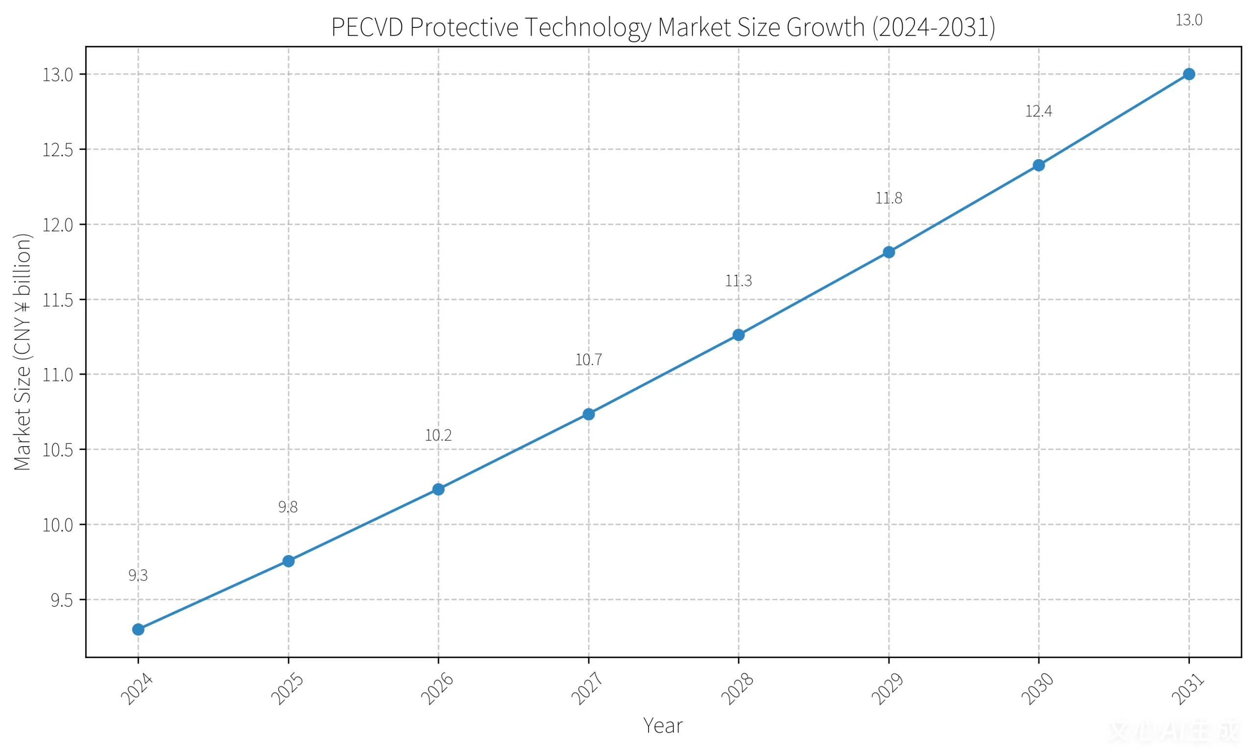
Market research indicates that the global market for protective materials for Flexible Printed Circuits (الشركة العامة للفوسفات) alone was approximately RMB 930 million in 2024 and is projected to reach nearly RMB 1.3 مليار من قبل 2031, with a compound annual growth rate (CAGR) ل 4.9%.
This reflects the sustained growth of the electronic device protection market, with plasma nano-coating technology capturing an increasingly significant share.
Future Development Trends
Plasma nano-coating technology is evolving toward multifunctionality, ذكاء, and environmental sustainability. New materials such as graphene-enhanced coatings and self-healing coating systems are emerging, offering expanded possibilities for PCB and PCBA protection.
Self-healing coating technology represents another frontier. Research shows that graphene-enhanced vitrimer coatings can achieve scratch repair and corrosion protection recovery after heating at 160°C for 3 ساعات, significantly extending the effective protective lifespan of products.
As electronic devices continue to miniaturize and integrate, with ever-increasing reliability demands, plasma nano-coating technology is set to become the preferred protection solution for high-end electronics, with its penetration in electronic manufacturing steadily rising.
As IoT devices trend toward miniaturization, plasma nano-coating technology is deeply integrating with materials science and smart manufacturing. في المستقبل, we can expect more innovative solutions, such as self-healing and photoresponsive coatings, to introduce new paradigms in electronic protection.
For electronics manufacturers seeking to enhance product reliability and market competitiveness, now is the ideal time to identify high-quality plasma nano-coating suppliers and evaluate their integration into production lines.

some really nice and useful information on this site, too I believe the design and style holds wonderful features.