
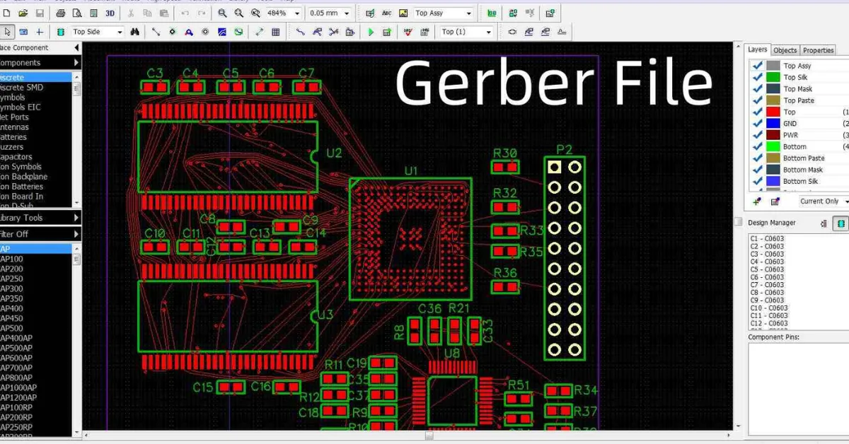
Introducción: Archivos Gerber: el ADN de la fabricación de PCB
En Diseño de PCB de alta velocidad, Los archivos Gerber encapsulan 90% de datos de fabricación. Según los estándares IPC-2581, 85% de global Fabricantes de PCB Confíe en Gerber como documentación de producción primaria. Como el “modelo industrial” de electrónica, Los archivos de Gerber describen precisamente la estructura física de una placa de circuito a través de la codificación en capas. Esta guía decodifica el significado de ingeniería de cada capa para ayudarlo a dominar fabricación de PCB.
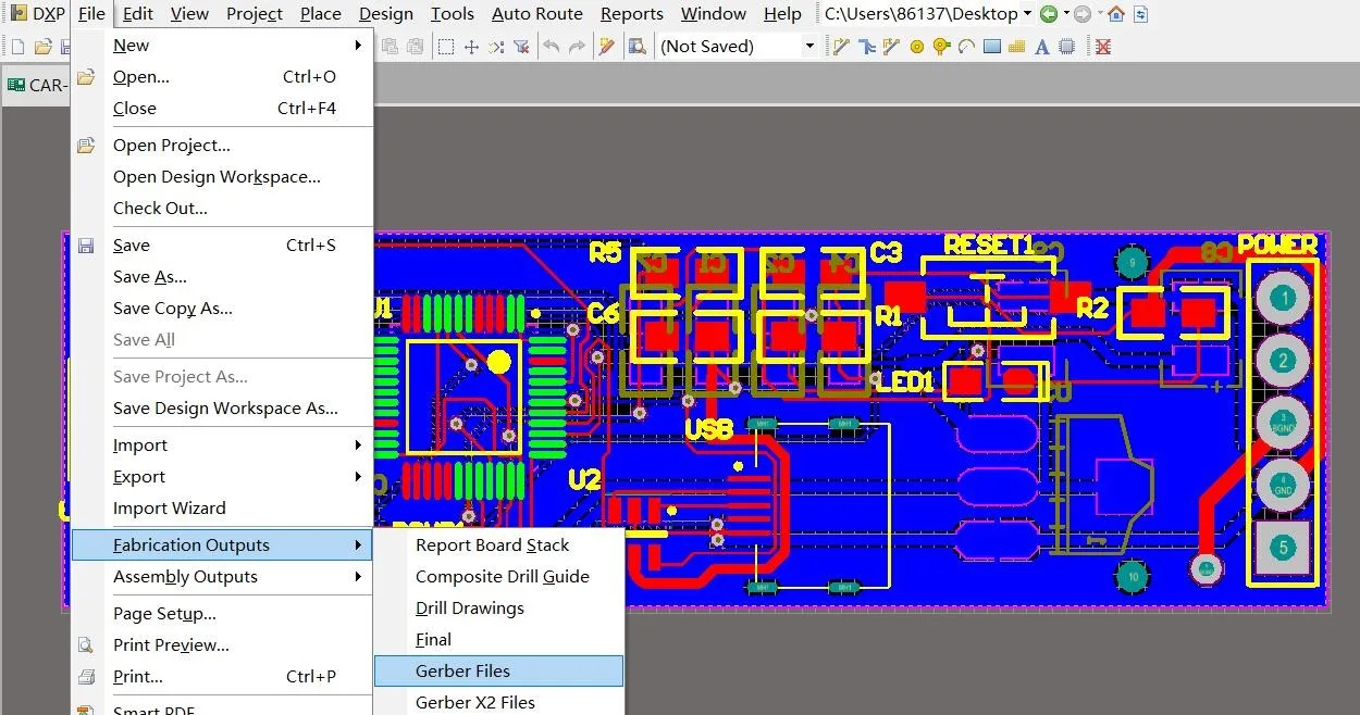
Sección 1: Complete el flujo de trabajo de exportación de archivos Gerber
1.1 Verificación previa a la exportación
-
Validación de la RDC: Asegurar el espacio entre el cumplimiento de las normas IPC-2221 (mín.. traza/espacio = 0.1 mm @ 6 capas PCB)
-
Confirmación de apilamiento: El control de impedancia debe satisfacer:

Dónde h = grosor dieléctrico, W. = Ancho de rastreo, t = grosor de cobre (1 Oz = 35 µm).
1.2 Comparación del modo de exportación
| Método | Caso de uso | Integridad del archivo |
|---|---|---|
| Exportación de un solo clic | Estándar 4-6 PCB de capa | 95% |
| Configuración personalizada | PCB HDI / Vías ciegos/enterrados | 100% |
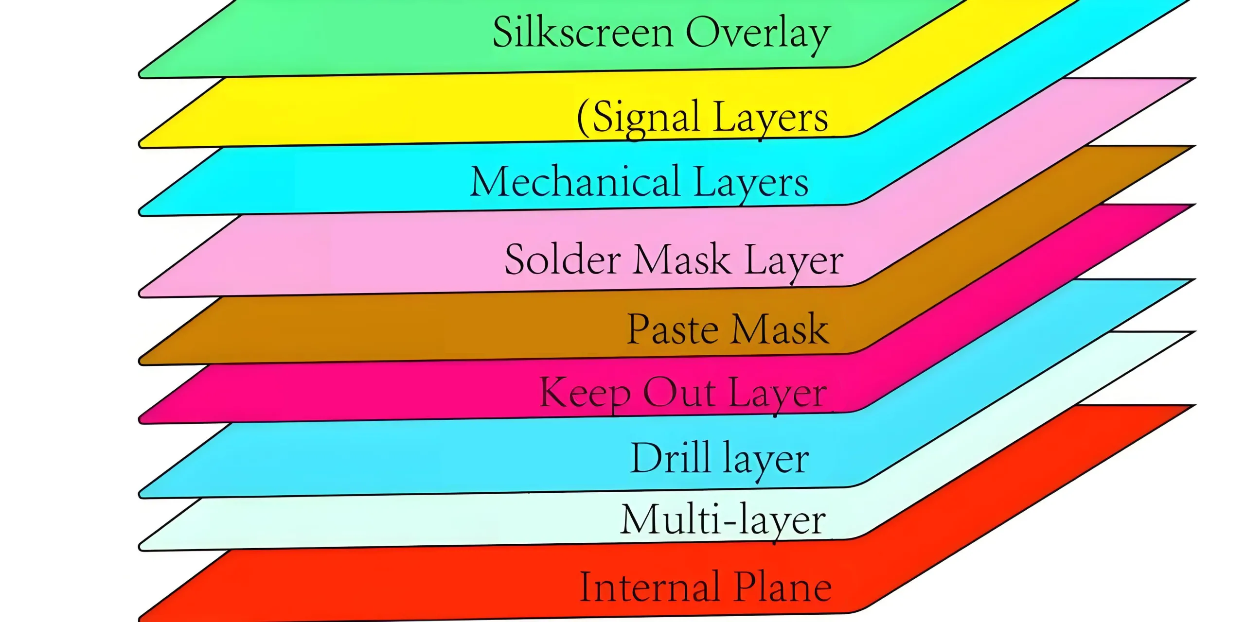
Sección 2: Estructura de la capa Gerber Dive Deep Dive
2.1 Capas conductoras explicadas
Capas de cobre:
-
Capa superior/inferior: Enrutamiento superficial (tipo. 1 onzas de cobre)
-
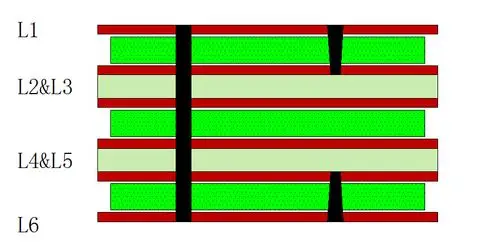
Capas internas: 6-apilamiento de PCB de capa: Top-gnd-señal-potencia-señal-bottom
Capas de perforación:
2.2 Capas de soporte de procesos
Capa de máscara de soldadura:
-
Salida de imagen negativa (Expone aberturas de cobre)
-
mín.. autorización: 0.07milímetros (Previene la falla de puente de máscara de soldadura)
Pegar la capa de máscara:
-
Aperture de plantilla = tamaño de almohadilla × 90%
-
Los paquetes QFN requieren un diseño de cuentas anti-Solder de puente cruzado
Capa de plisilla:
-
Altura de texto ≥0.8 mm, Ancho de línea ≥0.15 mm
-
La plantilla de la capa inferior requiere reflejo
Sección 3: Características de Gerber en PCB multicapa
3.1 Recuento de capas vs. Archivos gerber
| Capas de PCB | Archivos gerber | Requisitos especiales |
|---|---|---|
| 1-2 | 8-10 | A través de los agujeros estándar |
| 4-6 | 15-20 | control de impedancia + Vippo |
| 8+ | 25+ | Vias ciegos + apilamiento híbrido |
3.2 Implementación de procesos avanzados
Vippo (A través de):
-
Diámetro del orificio ≤0.15 mm, Tamaño de la almohadilla ≥0.3 mm
-
Etiquetar como “μvia” en capas de perforación
Diseño de ranura escalonada:
-
Anotación mecánica:
SLOT:3.0x1.2mm @ Layer2-4
Sección 4: Reglas de DFM impulsadas por datos de Gerber
4.1 Controles de fabricación
4.2 Marcadores de diseño de alta velocidad
-
Parejas diferenciales:
IMPEDANCE:100Ω±10% -
RF TRACES:
NO_SOLDERMASK(Reduce la variación DK)
Sección 5: Desde el ingeniero de diseño hasta el arquitecto de PCB
Verdadero maestro de expertos en diseño de PCBA:
5.1 Integridad de señal (Y)
-
Control de retraso: ΔL ≤ 0.05√ε_r (ps/pulgada)
-
Prevención de la diafonía: 3W Regla (Espacio ≥ 3 × ancho de rastreo)
5.2 Integridad de poder (PI)
-
Objetivo impedancia:

-
Diseño del condensador de desacoplamiento: Colocación radial por capacitancia
5.3 Gestión Térmica
-
Capacidad de corriente de cobre:
I = 0.048⋅ΔT0.44⋅A0.725
(ΔT = aumento de temperatura, A = sección transversal)
Conclusión: La filosofía de ingeniería de los archivos gerber
Al exportar datos de Gerber, recordar: Estos “frío” Las capas representan diálogos de precisión entre la electrónica y la ciencia de los materiales. Desde ejercicios láser de 0.05 mm a tolerancias de máscara de soldadura de 10 μm, Cada capa de Gerber narra la filosofía de ingeniería del aislamiento de la señal y las vías conductoras.
Los datos de la industria revelan: El uso de Gerber+ODB ++ Entrega de doble archivo aumenta el rendimiento de primer paso por 40%. En la era 5G/AI, Dominar la semántica de Gerber significa controlar el núcleo de la fabricación de hardware inteligente.


De hecho, haces que parezca tan fácil junto con tu presentación, sin embargo, creo que este tema es realmente una cosa que siento que de ninguna manera entendería.
Parece demasiado complejo y muy extenso para mí.
Estoy mirando hacia adelante en su publicación posterior, Intentaré entenderlo!
Me encantó tanto como recibirás que se lleva a cabo aquí.
El boceto es atractivo, Su tema es elegante.
sin embargo, Tú el comando tiene una impaciencia por encima de que deseas entregar lo siguiente.
sin duda, sin duda, vuelve a venir más anteriormente, ya que exactamente lo mismo casi muy a menudo dentro del caso
protege este aumento.