
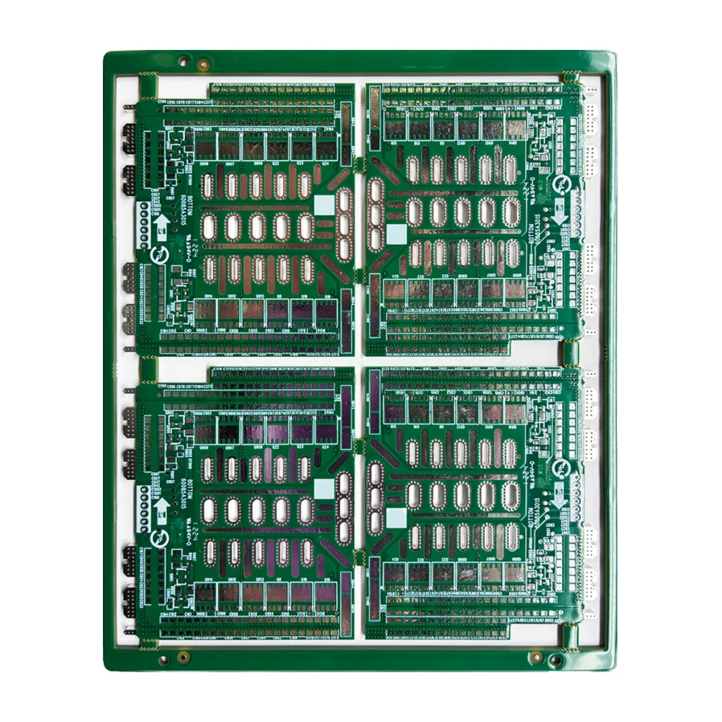
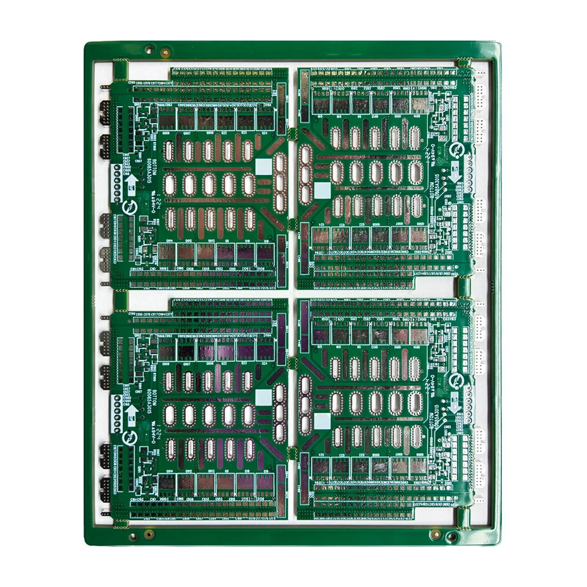
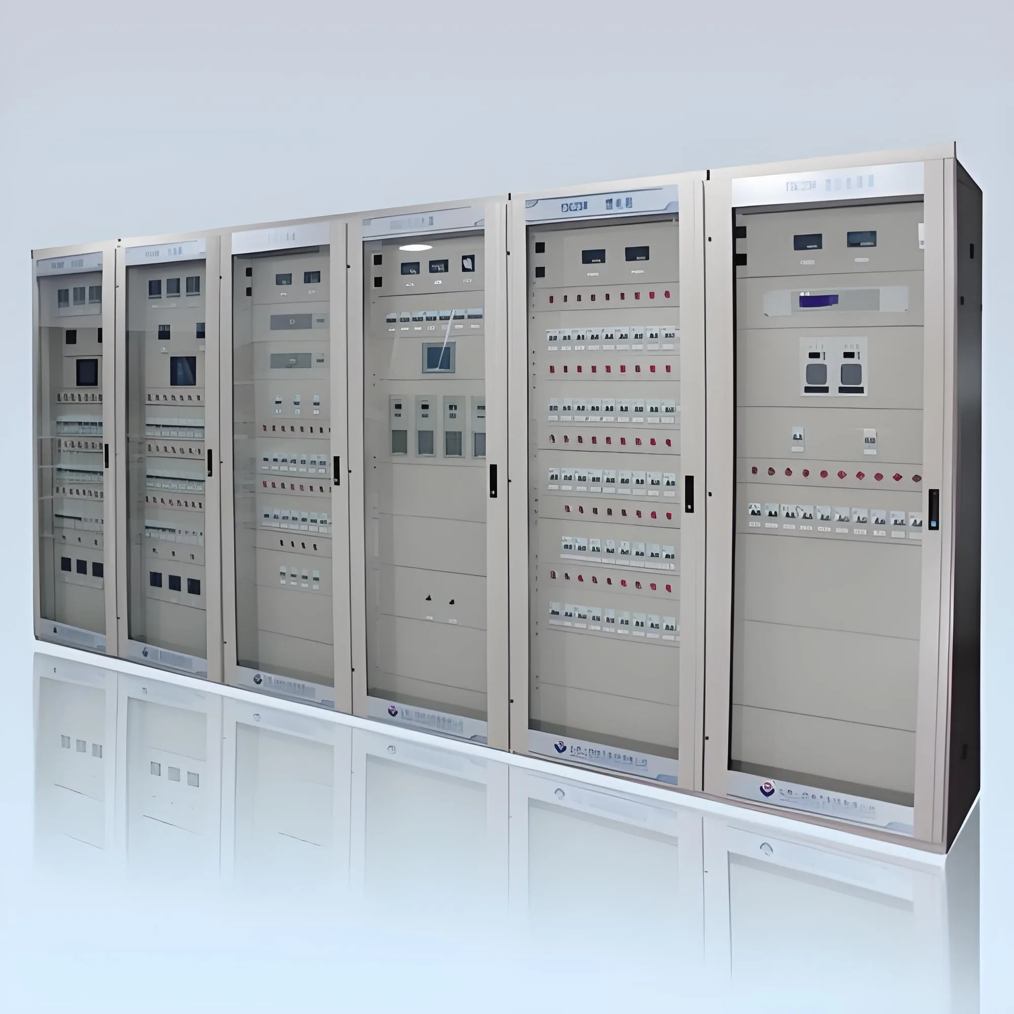
PCB rígido de 8 capas de alta confiabilidad Descripción general del producto & Definición
En el ámbito de la alta velocidad, diseño electrónico de alta densidad, PCB multicapa (Placas de circuito impreso) son indispensables. UGPCB 8-PCB rígido de capa, construido con una sustancial 2.0mm de espesor del tablero y 3Lámina de cobre pesada OZ, está diseñado para soportar entornos eléctricos y físicos exigentes. No solo sirve como base para la conectividad eléctrica, sino también como un componente crítico que garantiza la estabilidad del dispositivo y una mayor confiabilidad del producto.. Para aplicaciones en controles industriales., sistemas de energía, o electrónica automotriz, Esta placa de alta especificación es la solución óptima para complejos, diseños de alto rendimiento.
Especificaciones principales
-
Recuento de capas: 8-PCB rígido de capa
-
Grosor del tablero terminado: 2.0mm ±10%
-
Materia prima: FR-4, Temperatura de transición vítrea (tg) ≥ 170°C
-
Acabado superficial: Nivelación de soldadura por aire caliente sin plomo (HASL-LF)
-
Peso del cobre: 3 onzas por pie cuadrado (≈105μm) tanto para capas internas como externas
-
Máscara de soldadura & Platina: Máscara de soldadura LPI verde, Leyenda serigrafiada blanca
Consideraciones críticas de diseño
Al diseñar con esta PCB de alta especificación, Los ingenieros deben priorizar.:
-
Gestión Térmica: Aprovechar la alta capacidad de transporte de corriente de 3OZ cobre pesado para optimizar los planos de potencia y tierra, reduciendo la impedancia y el aumento de calor. Utilice la simulación térmica junto con la alta resistencia al calor de Material FR-4 TG170.
-
Control de impedancia & Integridad de señal: El apilamiento de 8 capas permite una separación efectiva de la señal, fuerza, y capas de tierra. Cálculo y control precisos de la impedancia de traza (p.ej., 50Ω de un solo extremo, 100Ω diferencial) Es esencial para minimizar la reflexión y la diafonía..
-
Mecánico & Fiabilidad eléctrica: El 2.0tablero de mm de espesor mejora la rigidez general, adecuado para aplicaciones con vibración o tensión de inserción. Para nodos de alto voltaje o alta corriente, ajuste el ancho de la traza y el espacio libre de acuerdo con Estándares IPC-2221 y el 3Peso de cobre en onzas para garantizar márgenes de seguridad.
-
DFM (Diseño para la fabricación): Colaborar con el equipo de ingeniería de UGPCB desde el principio para abordar requisitos específicos para PCB de cobre pesado y PCB de placa gruesa tratamiento, tales como parámetros de perforación y uniformidad del revestimiento, asegurando un proceso de fabricación de alto rendimiento.
Cómo funciona & Estructura
Un 8-PCB de capa se fabrica laminando múltiples capas conductoras en una sola unidad mediante procesos precisos que incluyen imágenes de la capa interna, laminación, perforación, y enchapado. Las conexiones eléctricas entre capas se establecen mediante orificios pasantes chapados (PTH), vias ciegas, o vías enterradas. Un ejemplo típico de acumulación es:
Capa superior (Señal) — Preimpregnado — L2 (Suelo) — Núcleo — L3 (Señal) — Núcleo — L4 (Fuerza) — Núcleo — L5 (Señal) — Preimpregnado — Capa inferior (Señal)
Este “sándwich” La estructura aísla eficazmente las señales de alta velocidad., proporciona planos de referencia sólidos, y garantiza una distribución eficiente de la energía.
Actuación & Características clave
-
Rendimiento eléctrico superior: 3OZ cobre pesado Proporciona una resistencia del conductor extremadamente baja y una excelente capacidad de transporte de corriente. (Más de 3 veces más que el cobre estándar de 1 oz.), reduciendo la pérdida de energía y la caída de voltaje.
-
Fiabilidad térmica excepcional: Material FR-4 TG170 de alta Tg Soporta temperaturas de operación y soldadura más altas.. Combinado con la conductividad térmica del cobre pesado., Mejora significativamente la confiabilidad a largo plazo en entornos de alta temperatura..
-
Estabilidad mecánica mejorada: El 2.0tablero de mm de espesor combinado con FR-4 rígido ofrece una resistencia superior a la flexión y la vibración., ideal para condiciones de funcionamiento duras.
-
Alta confiabilidad de las juntas de soldadura: El Acabado superficial HASL-LF proporciona un piso, Superficie de almohadilla coplanar con excelente soldabilidad y vida útil prolongada., Cumple con las directivas RoHS.
-
Interconexión de alta densidad (IDH) Capacidad: El diseño de 8 capas ofrece un amplio espacio de enrutamiento para circuitos complejos, Facilitar la miniaturización del dispositivo y la integración funcional..
Descripción general del proceso de producción
Revisión de ingeniería → Corte de materiales (FR-4 TG170) → Imágenes de la capa interna & Aguafuerte (3ONZ) → Tratamiento de óxido & Laminación → Perforación Mecánica & Revestimiento de cobre → Patrón de capa exterior & Enchapado (a 3OZ) → Aplicación de máscara de soldadura (IPV verde) & Platina (Blanco) → Acabado superficial HASL sin plomo → Pruebas eléctricas & Inspección final (según los estándares IPC)
Cada etapa incorpora estrictos puntos de control de calidad para garantizar que cada PCB multicapa de alta confiabilidad cumple con las especificaciones exactas del cliente.
Aplicaciones primarias & Casos de uso
Esta PCB está diseñada para alta potencia., aplicaciones de alta estabilidad:
-
Sistemas de control industriales: PLC, unidades de motor, y fuentes de alimentación industriales que requieren PCB de cobre pesado para alta corriente.
-
Energía renovable & Sistemas de energía: Inversores solares, Sistemas UPS, y módulos de carga para vehículos eléctricos que dependen de una alta capacidad de corriente y resistencia térmica.
-
Electrónica automotriz: Cargadores a bordo (OBC), Sistemas de gestión de baterías (Bms), y convertidores DC-DC, dónde PCB de alta Tg son esenciales para las temperaturas debajo del capó.
-
Infraestructura de Telecomunicaciones: Unidades amplificadoras de potencia de estación base y sistemas de energía de respaldo de red.
-
Prueba de alta gama & Equipo de medición: Instrumentos que requieren una entrega de energía estable y un rendimiento de bajo ruido..
Clasificación de productos (Según los estándares IPC)
-
Por recuento de capas: PCB multicapa (>4 capas), específicamente un 8-placa de circuito de capa.
-
Por rigidez: PCB rígido.
-
Por material base: FR-4 PCB, subconjunto: PCB TG alto (Tg ≥ 170°C).
-
Por Proceso Especial: PCB de cobre pesado (para IPC-2152), PCB de tablero grueso.
-
Por clase de aplicación: Adecuado para Clase IPC 2 (Productos electrónicos de servicio dedicado) y Clase 3 (Productos electrónicos de alta confiabilidad) aplicaciones, incluido PCB de grado industrial, PCB para electrónica de potencia, y PCB de grado automotriz.


