
UGPCB Double-Sided Gold-Plated PCB Product Overview
UGPCB’s gold-plated double-sided PCB board represents the pinnacle of accessibility and performance in tarjeta de circuitos tecnología. Designed for engineers and creators who demand reliability without the complexity of multi-layer boards, this product leverages the proven Immersion Gold (ACEPTAR) surface treatment to ensure robust connections and exceptional signal integrity. With a standard 1.2mm thickness, 1OZ copper cladding, and fine 6mil trace capabilities, it serves as the perfect substrate for a vast array of digital tarjeta de circuito impreso aplicaciones, from prototyping to full-scale production.
What is a Gold-Plated (Oro de inmersión) PCB de doble cara?
Definition and Basic Concept
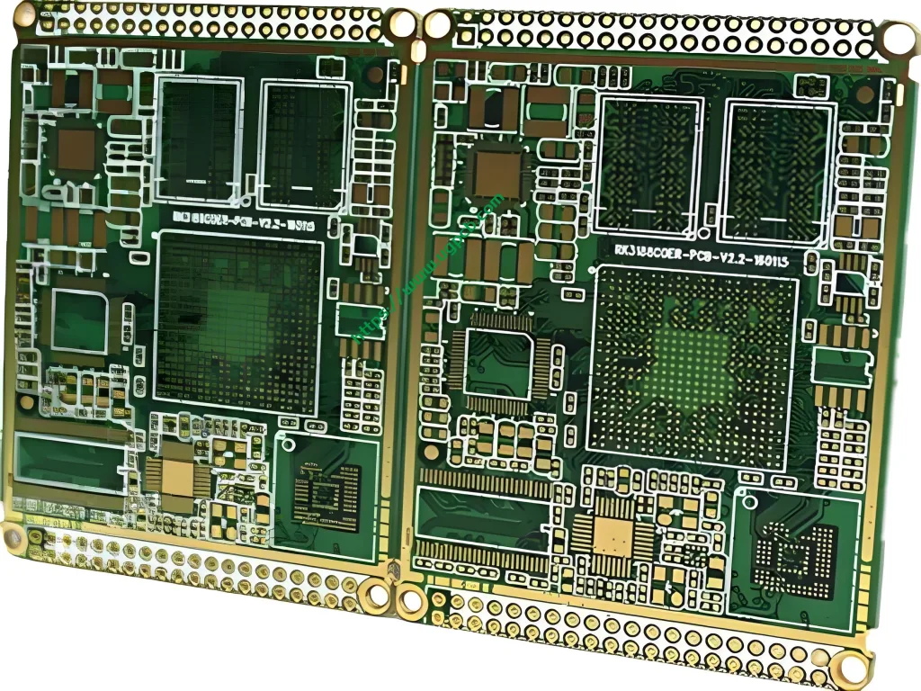
A PCB de doble cara is a circuit board that features conductive copper layers on both its top and bottom surfaces, allowing for more complex and dense circuit routing compared to single-sided boards. El término “gold-plated” in our context specifically refers to the Oro de inmersión (ACEPTAR) acabado superficial. This is a critical final step in the fabricación de PCB process where a thin layer of gold is chemically deposited over a nickel barrier layer on the copper traces. This combination provides a flat, oxidation-resistant, and highly solderable surface, making it ideal for double-sided PCB fabrication and subsequent Asamblea de PCBA.
In-Depth Specifications and Material Composition
The Building Blocks of Quality
The superior performance of our double-sided boards is rooted in the careful selection of materials and precise control of parameters:
-
Material central: High-quality FR4, a flame-retardant glass-reinforced epoxy laminate. This material offers an excellent balance of mechanical strength, aislamiento eléctrico, and cost-effectiveness.
-
Board Structure: 2 capas of copper foil, firmly bonded to the FR4 substrate.
-
Tratamiento superficial: Oro de inmersión (ACEPTAR). This process creates a flat surface crucial for modern components, protects the underlying copper, and provides a long shelf life.
-
Espesor de cobre: 1ONZ (approximately 35µm), a standard and robust weight that handles typical current loads in digital circuits effectively.
-
Espesor terminado: 1.2milímetros, offering a rigid and durable board structure for most applications.
-
Critical Design Rules: Minimum Trace/Space of 6mil (0.15milímetros), enabling a good level of design density for complex digital circuits.
-
Máscara de soldadura: Available in Green or White, providing insulation and protection against oxidation and solder bridges.
Key Advantages and Product Features: Why Choose UGPCB’s Immersion Gold PCB?
Unmatched Reliability and Performance
Choosing our gold-plated double-sided PCB translates to tangible benefits for your project:
-
Superior Flatness and Solderability: The ENIG finish is exceptionally flat, which is vital for reliably soldering fine-pitch components like BGAs and QFNs. This directly reduces defects in your tarjeta de circuito impreso proceso.
-
Excellent Oxidation Resistance: The gold layer is inert, preventing the copper from tarnishing over time. This ensures a reliable surface for soldering even after prolonged storage, making your prototipo de PCB and production inventory more manageable.
-
Stable Contact Surface for Connectors: The hard, durable gold surface is ideal for edge connectors and test points, providing a low-resistance, wear-resistant contact interface.
-
Dual-Sided Routing Capability: Effectively doubles the available area for routing traces compared to a single-sided board, allowing for more compact and efficient digital circuit board diseños.
-
Rentabilidad: For designs that don’t require the complexity of a 4-layer board, the double-sided PCB FR4 with ENIG finish offers the best performance-to-cost ratio for a wide range of applications.
Typical Applications and Use Cases: Where is This PCB Used?
Powering the Digital World
The versatility of our double-sided immersion gold PCB makes it a go-to solution across numerous industries:
-
Consumer Digital Electronics: Smart home controllers, IoT sensor nodes, dispositivos portátiles, and audio equipment.
-
Electrónica automotriz: Dashboard controllers, módulos de sensores, and lighting control units.
-
Sistemas de control industriales: PLC I/O modules, unidades de motor, and measurement instrumentation.
-
Telecomunicaciones: Routers, interruptores, and network interface modules.
-
Dispositivos médicos: Patient monitoring equipment and diagnostic tools where reliability is paramount.
-
Prototyping and R&D: The ideal choice for functional prototipos de PCB that closely mimic final production performance.

The Manufacturing Workflow: A Glimpse into Precision Engineering
Del diseño a la entrega
The production of a high-quality double-sided PCB is a meticulous process:
-
Preparación de material & Perforación: The FR4 panel is prepared, and via holes are precision-drilled to create interconnections between layers.
-
Plating Through Hole (PTH): A conductive layer is chemically deposited inside the drilled holes to establish electrical connectivity between the two sides.
-
Pattern Imaging & Desarrollo: The circuit pattern is transferred onto the copper layers using photoresist and UV light.
-
Aguafuerte: Unwanted copper is chemically etched away, leaving behind the desired circuit traces.
-
Aplicación de máscara de soldadura: The green or white solder mask is applied and cured, exposing only the component pads and vias.
-
Acabado de superficies – Oro de inmersión: The board undergoes the ENIG process, applying the nickel barrier and thin gold layer.
-
Impresión de plisabra: Component designators and logos are printed on the board.
-
Prueba eléctrica & Inspección final: Each board is rigorously tested for continuity and short circuits to ensure 100% functionality before shipment.

Design Considerations and Best Practices
Optimizing Your Board for Success
To fully leverage the capabilities of this PCB de doble cara, consider these design tips:
-
Utilize Vias Effectively: Strategically place vias to create short and efficient signal return paths between layers.
-
Power Plane Strategy: While a full ground plane is ideal, you can use generous copper pours on both sides to create a stable power distribution network for your digital PCB.
-
Respect the 6mil Rule: Adhere to the minimum trace and space requirements to ensure manufacturability and yield.
-
Colocación de componentes: Place critical and noise-sensitive componentes on one side (typically top) to simplify routing and minimize interference.
Conclusión: Your Trusted Partner for High-Quality PCBs
UGPCB’s gold-plated double-sided PCB board is more than just a component; it’s a reliable foundation for innovation. By combining the robust FR4 material, the advanced Immersion Gold surface treatment, and our commitment to precision manufacturing, we provide a product that balances performance, durabilidad, y costo. Whether you are a startup working on a prototipo de PCB or an established company scaling up Asamblea de PCBA, this board is engineered to meet the rigorous demands of the modern digital world.
Listo para iniciar tu proyecto? [Get an instant quote today!] o [Contact our PCB experts for a design review.]


