
1. Market Background: Why Automotive Electronics Need High‑Reliability PCBs
Modern electric vehicles and ADAS systems use more electronic parts every year.
Data from China Commercial Industry Research Institute shows: China’s automotive electronics market reached USD ~169 billion in 2024, と 10.95% year‑on‑year growth. This demand pushes engineers to replace traditional rigid プリント基板 + wire harnesses with more compact and reliable solutions.
あ rigid‑flex PCB combines the stability of rigid boards with the bendability of flex circuits.
Industry studies show that switching to rigid‑flex can:
-
Save ~40% installation space
-
Reduce vibration‑related failures by ~65%
-
Lower BOM cost by ~22% through higher integration
The global automotive rigid‑flex PCB market is expected to exceed USD 5 10億 2025.
UGPCB designed the 自動車用PCB (HDI R‑FPCB) – a high‑density interconnect rigid‑flex board that meets ISO 26262 and IPC‑6012DA Class 3 要件. It is the ideal choice for your automotive rigid‑flex PCB prototype.
2. 製品の定義 & 科学的分類
2.1 製品名 & モデル
-
製品名: 自動車用PCB (HDI R‑FPCB) – Automotive‑Grade Rigid‑Flex HDI PCB
-
Model Code: HDI R‑FPCB 1+2+1 構造
-
Focus Keyword: Automotive rigid‑flex PCB prototype (Yoast SEO focus keyword)
2.2 科学的分類 (Based on IPC & UL Standards)
| Classification Method | 標準 | カテゴリ |
|---|---|---|
| By structure | IPC‑2223 | Rigid‑Flex Multilayer Board (≥3 conductive layers) |
| By HDI technology | IPC‑2226 | Type III – 2‑step HDI with “1+2+1” stackup, laser microvias |
| By performance class | IPC‑6013 | クラス 3 (high‑reliability, continuous operation) |
| By application | - | Automotive electronics – ECU, アダス, BMS, infotainment |
2.3 主要なパラメータ (Quick Reference Table)
| パラメーター | 仕様 |
|---|---|
| モデル | 自動車用PCB (HDI R‑FPCB) |
| 材料 | FR‑4 + PI (ポリイミド) |
| Layer stackup | 1+2+1 (2‑step HDI rigid‑flex) |
| ソルダーマスクの色 | 緑 / 白 |
| 仕上げた厚さ | 1.2 mm |
| 銅の厚さ | 0.035 mm (1 オズ) |
| 表面仕上げ | わずか2U” (エレクトロレスニッケルイマージョンゴールド) |
| 分. 線幅 / 間隔 | 0.1 mm / 0.1 mm |
| 応用 | Automotive electronics rigid‑flex PCB prototype |
テーブル 1 – Core specifications of UGPCB Automotive PCB (HDI R‑FPCB).
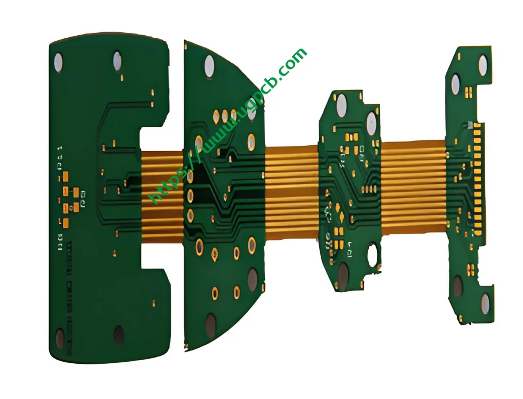
3. Stackup & 構造: “1+2+1” 2‑Step HDI Rigid‑Flex
3.1 The 1+2+1 Stackup Explained
これ automotive rigid‑flex PCB prototype features a 1+2+1 HDI build‑up:
-
層 1 – Outer rigid layer (component mounting & ルーティング)
-
層 2 – 1st HDI build‑up (埋葬された / blind microvias)
-
層 3 – Core layer (contains PI flex area)
-
層 4 – 2nd HDI build‑up
-
層 5 – Outer rigid layer (bottom side routing & はんだ)
The flex area stays on the PI core and opens through the rigid coverlay. This design gives you both high routing density (HDI PCB) and 3D bendability (rigid‑flex PCB).
3.2 HDI Classification per IPC‑2226
IPC‑2226 defines HDI by: line width/spacing ≤ 100 μm, microvia pad < 400 μm, and density > 20 pads/cm².
私たちの 0.1 mm line/space meets the standard. Laser microvias enable the 1+2+1 structure as タイプII (2‑step HDI) – ideal for automotive electronics.
| HDI Type (IPC‑2226) | Build‑up Feature | Typical Application |
|---|---|---|
| タイプI (1‑step) | Single microvia layers on core | 家電 |
| タイプII (2‑step) | Two build‑up layers per side | 自動車, 工業用, high‑end devices |
| タイプIII (≥3‑step) | Any‑layer interconnect | Flagship smartphones |
3.3 材料: FR‑4 + PI
-
Rigid areas (FR‑4) – Epoxy glass woven fabric. Provides strong mechanical support for heavy components (コネクタ, large ICs).
-
Flex area (PI) – Polyimide film (FCCL). TG > 260℃, UL 94 V‑0 rated. Withstands engine‑bay temperatures.
The CTE (coefficient of thermal expansion) difference between PI (16–20 ppm/°C) そして FR‑4 (14–18 ppm/°C) 重要です. UGPCB controls lamination parameters to avoid delamination from –40°C to +125°C thermal cycling.
4. Design Guidelines for High‑Performance Rigid‑Flex HDI PCBs
4.1 Fine Line & 空間 (0.1 mm / 0.1 mm)
達成 0.1 mm trace/space with 1 OZ copper allows 50% higher routing density than 0.15 mm designs.
For automotive プリント基板 later assembly, follow these rules:
-
インピーダンス制御 – Match differential pair impedance (90 おお / 100 おお) across both FR‑4 and PI zones.
-
長さの一致 – Keep intra‑pair mismatch < 0.5 mm on flex area because PI’s Dk (3.4–3.5) differs from FR‑4 (4.2–4.5).
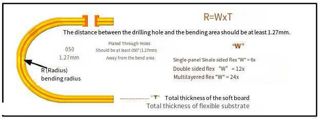
4.2 半径の計算を曲げます (IPC‑2223)
Rigid‑flex PCBs must respect minimum bend radii for reliability.
According to IPC‑2223 and industry practice:
Rmin, static=(6 に 12)×tflexRmin, dynamic≥10×tflex
どこ tflex = total flex area thickness (銅 + coverlay).
For a typical 0.2 mm flex stack, the static minimum radius is 1.2–2.4 mm. UGPCB recommends R ≥ 6 mm for dynamic bending in door hinges or seat adjusters.
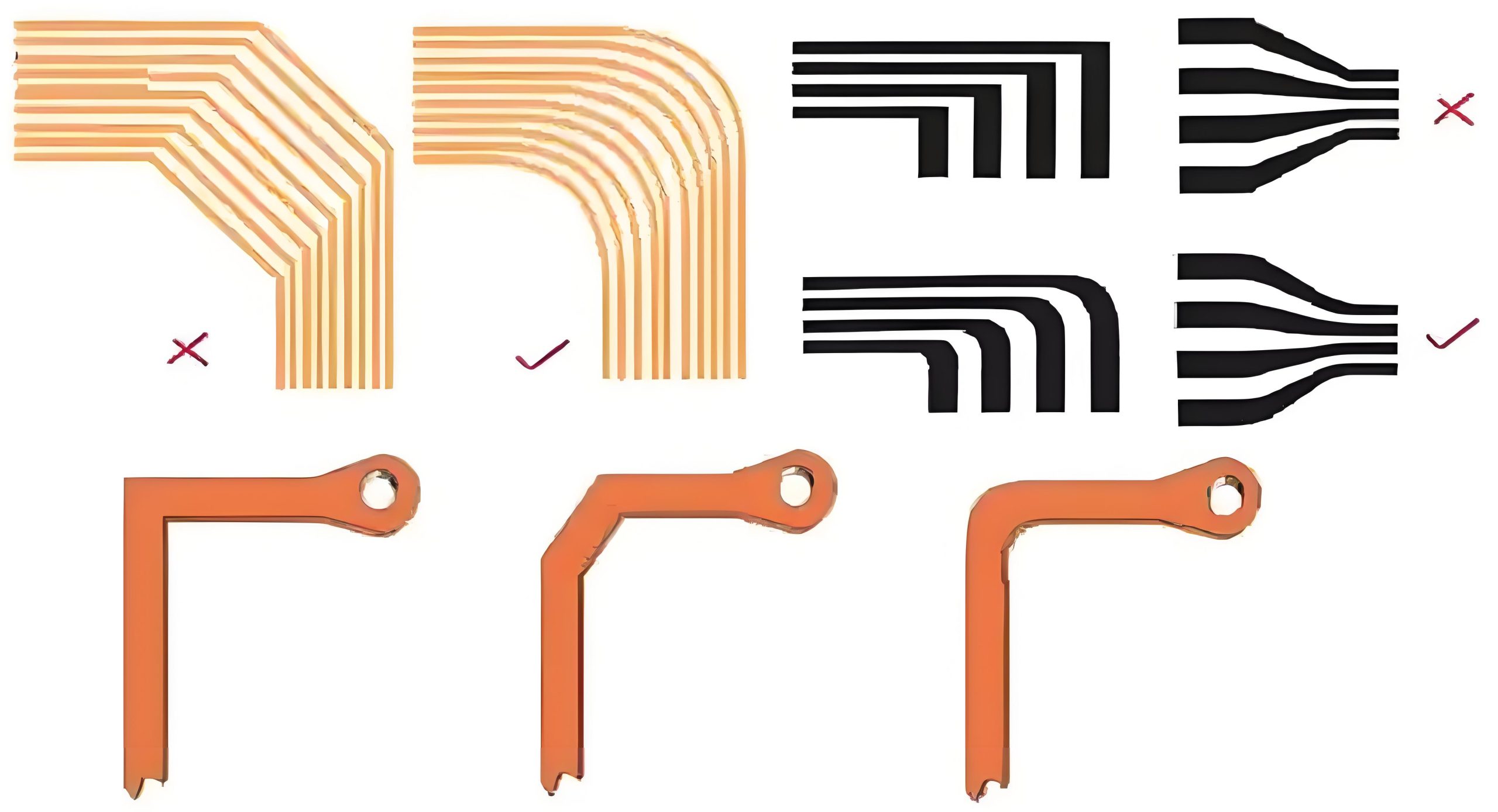
4.3 Rigid‑Flex Transition Zone – Key Points
-
45° tapered interface – Avoids stress concentration.
-
Route traces parallel to bend axis – Never cross the bend area perpendicularly.
-
Teardrop pads & rounded coverlay openings – Distribute mechanical stress.
-
使用 0.5 OZ copper on high‑flex zones - 1 OZ is stronger but less flexible.
5. 製造工程の流れ (ISO & IPC Compliant)
UGPCB follows IPC‑6013D for rigid‑flex qualification. 重要な手順:
-
Inner layer imaging – FR‑4 core and PI flex layer separately. AOI checks 0.1 mm lines.
-
レーザー掘削 (盲目 / buried microvias) - CO₂ laser removes FR‑4; UV laser for < 50 µm holes.
-
デスミア & electroless copper – Activates hole walls for plating.
-
Via filling & panel plating – Blind vias filled with copper (無効レート < 5%).
-
Sequential lamination – Builds the 1+2+1 stack in two steps. Flex area is masked during rigid layer lamination.
-
外層 & はんだマスク – Green or white LPI solder mask applied.
-
わずか2U” 表面仕上げ – IPC‑4552 compliant: 3–7 µm Ni + ≥0.05 µm Au. Double gold thickness for corrosion resistance.
-
ルーティング & 電気試験 - 100% flying probe or fixture test.
6. パフォーマンス & Reliability Data (IPC‑TM‑650)
| テスト | 状態 | 要件 | 標準 |
|---|---|---|---|
| Dielectric withstanding voltage | ≥1000 VDC | No breakdown | IPC‑TM‑650 2.5.7 |
| 絶縁抵抗 (normal) | ≥10^11 Ω | 合格 | IPC‑TM‑650 2.5.3 |
| サーマルサイクリング | –40°C ↔125°C, 1000 サイクル | No delamination, ΔR < 10% | IPC‑TM‑650 2.6.7 |
| Damp heat | 85℃ / 85% rh, 1000h | IR ≥ 10^9 Ω | IPC‑6013 Class 3 |
| Vibration | 10–2000 Hz, 20g, 4h/axis | No intermittent opens | ISO 16750‑3 |
| 動的曲げ | r = 5 mm, 5000 サイクル | No open circuit | 業界標準 |
All tests follow IPC‑TM‑650 methods and IPC‑6013 Class 3 要件.
7. 主な特長 & アプリケーションシナリオ
7.1 Why Choose This Automotive Rigid‑Flex HDI PCB
-
1+2+1 HDI + rigid‑flex – High density plus bendability.
-
0.1 mm line/space – Supports BGA pitch ≤ 0.5 mm.
-
UL 94 V‑0 – Flame retardant (extinguishes within 10 秒).
-
わずか2U” – Double gold thickness for 10–15 year automotive life.
-
Quick‑turn prototype – Samples ready in 7–10 days.
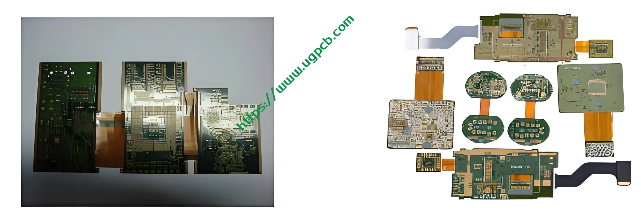
7.2 Typical Use Cases for Your Automotive Electronics PCB Prototype
-
ECU (エンジンコントロールユニット) – Sensor signals integrated directly on PI flex, eliminating connectors.
-
ADAS domain controller – Radar / camera modules need high‑speed signals and folding structures.
-
Infotainment system – Replace FPC + BTB connectors with one rigid‑flex PCB.
-
BMS (バッテリー管理システム) – Stacked voltage/temperature channels with UL 94 V‑0 compliance.
-
Automotive camera module – Flex section bends through door hinges without wire harness.
8. Why Partner with UGPCB for Your Automotive Rigid‑Flex PCB Prototype?
-
IPC member + UL certified – Full compliance with IPC‑6012DA & IPC‑6013D.
-
16,000 m² modern plant – Annual capacity 600,000 m², dedicated HDI production line.
-
Free DFM review - 15+ years average experience. UGPCB helps you optimize stackup and bend radius.
-
Fast prototype delivery – 7–10 days for rigid‑flex samples.
-
Free engineering consultation – CTE mismatch analysis, impedance tuning, and SMT assembly advice.
9. Get a Quote – Start Your Automotive Rigid‑Flex HDI PCB Prototype Today
Submit your Gerber files or share your technical requirements. UGPCB responds within 2 hours with a free stackup recommendation and price estimate.
Contact us now – simply fill in the brief form below:
-
Company name
-
電話 / 微信 / ワッツアップ
-
Design needs or target budget
UGPCB helps you build high‑reliability, high‑integration automotive electronics – one rigid‑flex PCB at a time.
Declaration
All specifications and data in this document are based on IPC‑2223, IPC‑2226, IPC‑6013, UL 94, and publicly available market reports (China Commercial Industry Research Institute, 2025). UGPCB reserves the right to update technical data. Please contact UGPCB sales for the latest engineering guidelines.


