
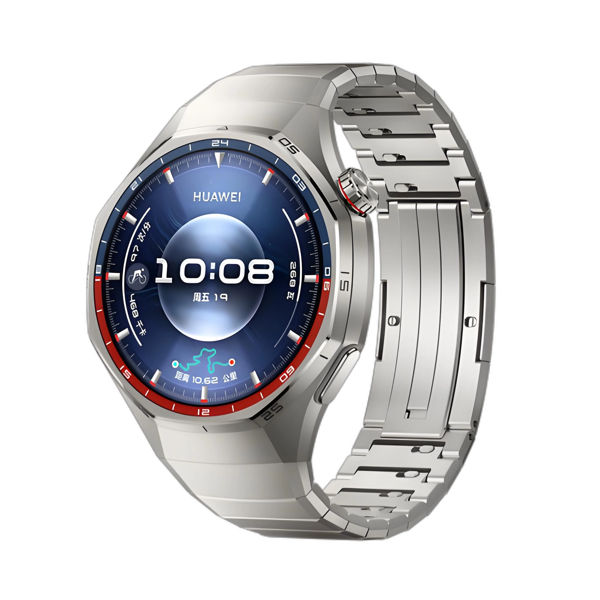
Engineers need compact designs and reliable connections for smart wear.
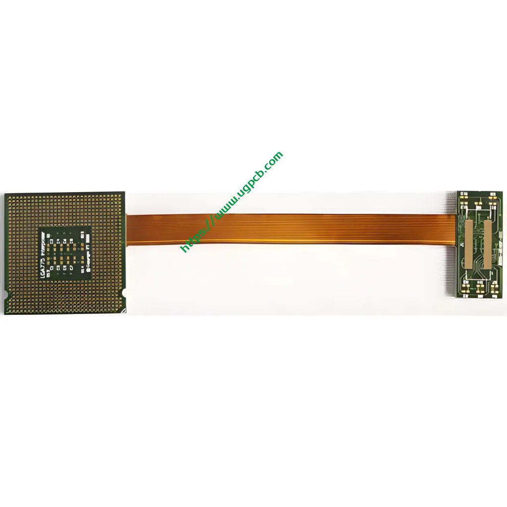
UGPCB の導入 Model 8L Smart Wear Rigid-Flex PCB (R-FPCB). This board combines 6 rigid layers and 2 flexible layers. It solves space and bending challenges in wearable プリント基板.
1. What Is a Smart Wear Rigid-Flex PCB?
あ リジッドフレックスPCB has both rigid sections (for soldering components) and flexible sections (for 3D interconnection).
私たちの 8L Smart Wear R-FPCB works perfectly for smartwatches, health patches, and AR glasses.
The 6 rigid layers support high-density wiring. The 2 flexible layers allow free bending.
This design replaces board-to-board connectors and flat cables. It eliminates contact failures common in tiny devices. It also improves shock resistance by removing mechanical joints.
2. 科学的分類
Based on IPC-6013 (Qualification and Performance Specification for Flexible Printed Boards), this product falls under:
-
タイプ: クラス 3 (high-reliability – medical/military/wearable) multilayer rigid-flex.
-
工事: Asymmetric (6 硬い + 2 flex).
-
Application level: Consumer high-reliability wearables.
3. 材料 & Stack-Up: Why PI + FR4?
We select materials based on physical properties and thermal stability.
Rigid Area – FR4
We use TG 170 FR4 (高いガラス転移温度). It keeps low Z-axis expansion during multiple reflow cycles. This ensures high BGA soldering yield.
Flexible Area – Polyimide (PI)
We use Polyimide film for the flex layers. PI has a low dielectric constant and wide working temperature (-200°C to +300°C). It allows over 100,000 bending cycles without cracking. This is critical for フレキシブル プリント基板 in wearables.
Stack-Up Construction
The flexible layers (L1/L2) embed inside the rigid section. We use stepped lamination at the transition boundary to spread mechanical stress.
Design rule: Never place vias in the bending area. That prevents micro-cracks from stress concentration. Our design follows this IPC-2223 rule strictly.
4. 主なパフォーマンス & Design Parameters (IPC-2223 Compliant)
The table below shows critical specifications for the 8L wearable rigid-flex board.
| パラメーター | UGPCB 8L R-FPCB Value | Design Insight |
|---|---|---|
| 層構造 | リジッド6L + フレックス2L | Asymmetric stack needs special compensation to avoid warpage |
| 仕上がり厚さ | 1.2mm (rigid zone) | Optimized for controlled impedance – meets IPC Class 2/3 |
| 最小トレース / 空間 | 3ミル / 3ミル | HDI capability – fits narrow bezel designs |
| Min Mechanical Hole | 0.2mm | Increases routing density |
| 銅の厚さ | 1 オンス (inner & outer) | Supports high charging currents |
| 表面仕上げ | イマージョンゴールド (同意する) | 2 microinches gold thickness |
5. Why Choose UGPCB for Your Wearable PCB Project?
あ. No More Flex Breakage
Wearable devices bend repeatedly (例えば。, watch straps). We use adhesiveless base material on the flex area. We also apply arc routing instead of 45° traces.
Data from our lab: Arc routing improves copper stress distribution by 40% compared to angled traces. This eliminates fatigue fractures.
B. Immersion Gold for Sweat Resistance
We finish the surface with 同意する (イマージョンゴールド), 2 microinches thick.
なぜ? Sweat and humidity corrode exposed copper. ENIG provides a flat pad surface (better than OSP) and excellent corrosion resistance. It also supports direct contact for buttons.
C. Strong Signal Integrity
Smart wear PCBs need clean Bluetooth and Wi-Fi signals. 私たちの 6 rigid layers include dedicated power and ground planes. These provide a complete return path for RF signals. That reduces electromagnetic interference (エミ) to a minimum.
6. 製造工程 & 品質管理
UGPCB uses automated lines to ensure high yield for the 8L rigid-flex PCB.
-
Material cutting & 掘削 - UV laser drills 0.2mm micro-vias in PI film.
-
デスミア & electroless copper – Plasma cleaning removes resin residue from holes.
-
Circuit patterning - LDI (レーザー直接イメージング) creates 3mil/3mil traces accurately.
-
ラミネート加工 – Low-flow prepreg controls resin bleed at the rigid-flex junction.
-
表面仕上げ – Strict chemical control for even ENIG deposition.
7. アプリケーション: Where This Rigid-Flex PCB Excels
これ R-FPCB fits devices that need both density and bending:
-
スマートウォッチ & fitness bands – connect main board to side buttons and heart-rate sensors.
-
TWS earbuds – fit into curved stems and hinge areas.
-
Medical monitoring patches – ultra-thin, skin-conforming flexible circuits.
-
Smart glasses – link left and right arms around the hinge.
 8. 規格 & Reliability Data
We design and test this wearable PCB according to international specifications:
-
Design standard: IPC-2223 (Flexible Printed Board Design)
-
Performance test: IPC-6013 (Flexible Board Qualification)
-
Reliability validation (UGPCB lab):
-
10 reflow cycles (peak 260°C) – no delamination
-
1000 hours damp heat (85℃ / 85% rh) – no corrosion
-
100,000 dynamic bends – no trace crack
-
9. Get a Quote – Start Your Wearable Project Today
UGPCB offers prototyping and mass production. We understand your timeline and quality needs for smart wear PCBs.
Send us your Gerber files or schematics. Our engineers will reply within 24 hours with:
-
あ DFM (製造用のデザイン) 報告
-
A competitive quote
[Call-to-action: Request Quote / Contact Sales]


