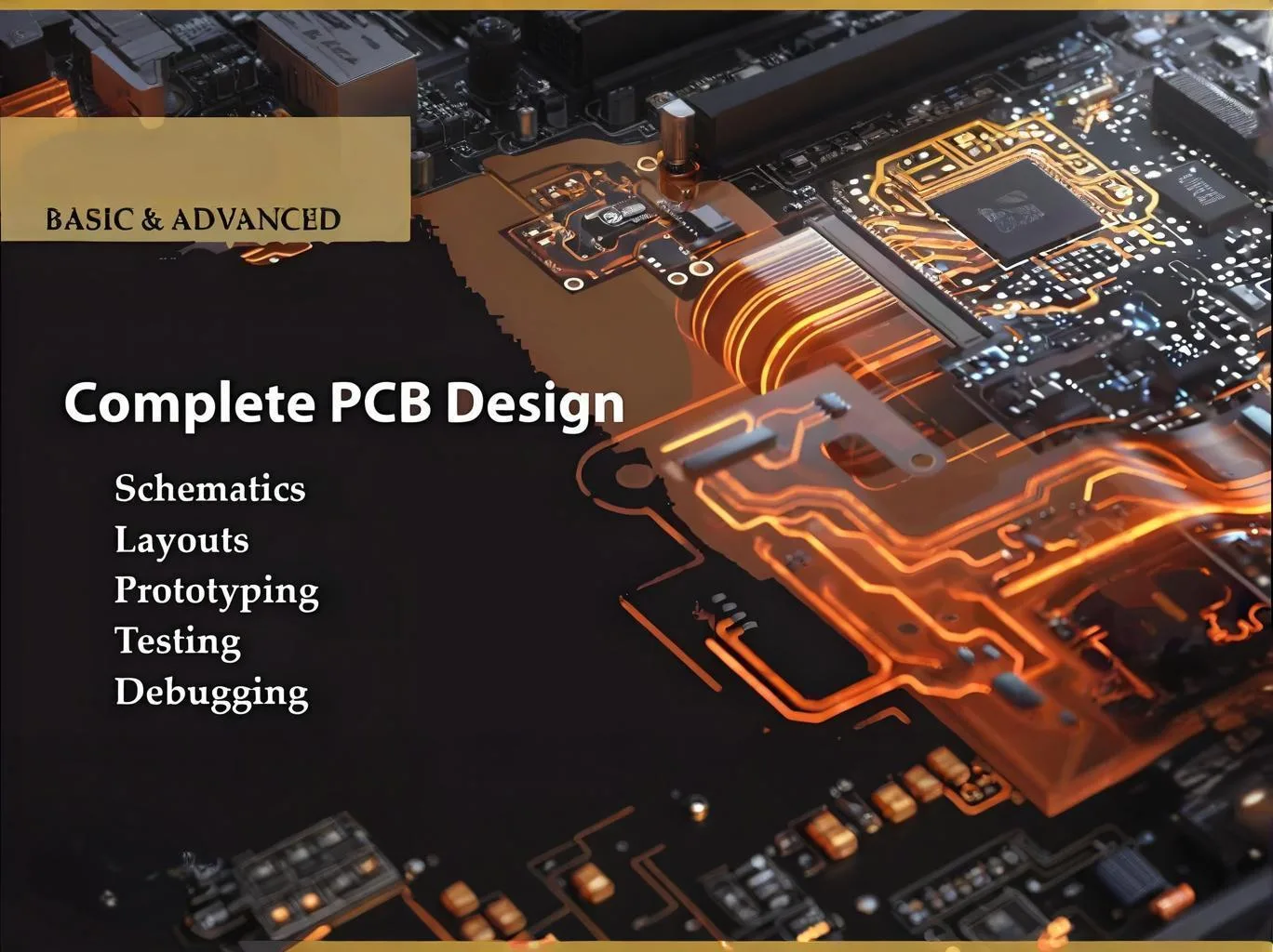
PCB 디자인의 예술과 과학: UGPCB가 회로 기판 연금술을 마스터하는 방법
(회로도부터 기능성 PCBA까지 엔지니어링 우수성)
12레이어 서버 마더보드에서 잘못 배치된 단일 경유로 인해 한때 기술 대기업의 비용이 발생했습니다. $2.3 백만 건의 리콜. UGPCB의 심천 R에서&D 센터, 엔지니어들은 고해상도 열화상 카메라를 통해 살펴봅니다., 이러한 재앙을 방지하기 위해 마이크로미터 정밀도로 트레이스 폭을 조정합니다..
오버 2000+ 연간 PCB 설계 프로젝트 항공우주를 가로질러, 의료, 그리고 5G 부문, UGPCB 개념적 설계도를 제조 가능한 걸작으로 변환합니다.. 그들의 비밀? 융합 10+ 년 전문 지식 및 군사급 설계 프로토콜을 달성합니다. 제로 실패율 미션 크리티컬 애플리케이션에서.
1. 전략적 과제: PCB 설계가 제품 성공을 좌우하는 이유
~ 안에 2024, 68% 전자제품의 고장 다시 추적 PCB 레이아웃 결점 (IPC 보고서). UGPCB의 설계 철학은 회로 기판을 다음과 같이 취급합니다. 기능성 조각품 어디:
-
90° 트레이스 코너마다 EMI가 다음과 같이 증가합니다. 3-5DB
-
0.1잘못된 정렬을 통해 mm는 다음과 같이 56Gbps 신호를 저하시킬 수 있습니다. 40%
-
적절한 열 설계로 구성 요소 수명이 연장됩니다. 2.3엑스
“PCB 설계는 선을 그리는 것이 아니라 전자 고속도로를 조율하는 것입니다”
— UGPCB 수석 설계 엔지니어
경제적 영향은 엄청나다:
-
DFM (제조 설계) 통합으로 인해 프로토타입 비용이 절감됩니다. 65%
-
일찍 신호 무결성 시뮬레이션 리스핀을 잘라냅니다. 80%
-
UGPCB의 표준화된 스택업 템플릿은 다음과 같이 출시 시간을 단축합니다. 4 주
2. UGPCB의 장점: 엔지니어링 DNA 해독
2.1 정밀하게 제작된 디자인 생태계
UGPCB 삼중 검증 작업 흐름 업계 벤치마크 설정:

하드웨어 전문화:
-
56Gbps PAM4 백플레인 디자인
-
0.2MM 피치 BGA 라우팅
-
20+ 층 HDI 보드 ~와 함께 0.1mm microvias
-
RF-디지털 하이브리드 레이아웃 (6GHz+)
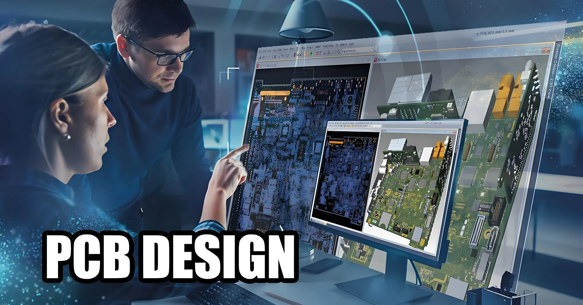
2.2 최첨단 도구 무기고
| 소프트웨어 | 기능 | UGPCB 구현 |
|---|---|---|
| 케이던스 SPB 16.6 | 3DEM 시뮬레이션, 제약 기반 라우팅 | 서버 마더보드 설계 |
| Altius 디자이너 23 | 통합 ECAD/MCAD 통합 | 웨어러블 의료기기 |
| 지멘스 Xpedition | 멀티보드 시스템 계획 | 자동차 제어 장치 |
| 독자적인 Thermal AI | 예측 핫스팟 매핑 | 고전력 산업용 컨트롤러 |
3. 회로 변환의 연금술: UGPCB의 설계 프로세스
3.1 컨셉 인큐베이션 단계
-
요구사항 해체: 클라이언트 사양을 다음으로 변환 23-포인트 기술 매트릭스
-
타당성 분석: 교차 확인 IPC-2221 표준
-
위험 완화 청사진: 깃발 97% 제조 가능성 문제 사전 레이아웃
3.2 도식 합성 마법
UGPCB 엔지니어가 활용:
-
구성 요소 인텔리전스 데이터베이스: 500k+ 검증된 발자국
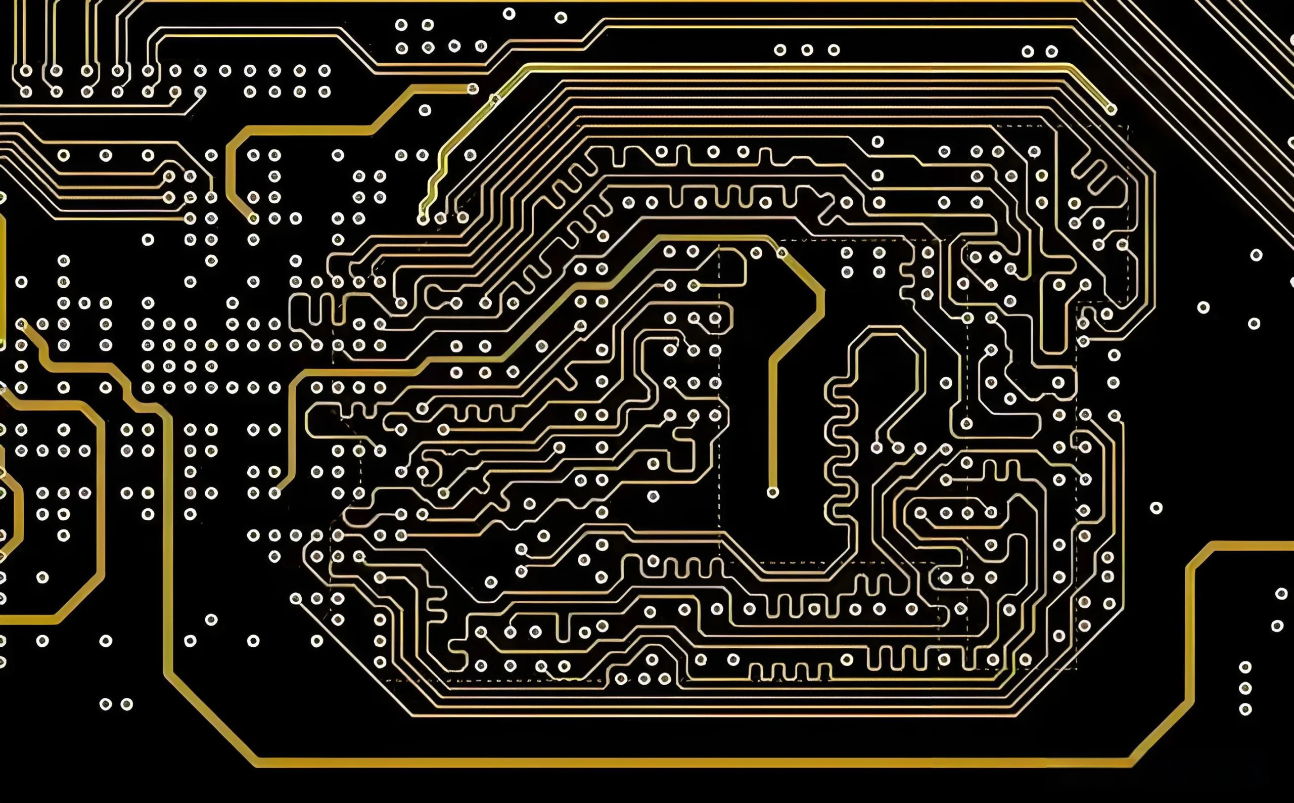
-
임피던스 제어 방식:
![]()
(UGPCB를 통해 달성 가능 13-레이어 스택업 라이브러리)
-
전력 무결성 모델링:

3.3 레이아웃 안무
중요한 규칙 시행:
-
3W 원리: 추적 간격 = 3× 트레이스 폭 누화 제어를 위해
-
10° 규칙: 피하다 직각 굴곡 ~에 >2GHZ 신호
-
열 완화 패턴: 4-QFN 패드용 스포크 연결
4. 제조 준비가 완료된 설계: 예술과 물리학이 만나는 곳
4.1 DFM/DFA/DFT 트리니티
UGPCB의 설계 검사에는 다음이 포함됩니다.:
| 검문소 | 기준 | UGPCB 향상 |
|---|---|---|
| 솔더 마스크 슬라이버 | >0.08mm 간격 | 레이저 정의 0.05mm 공차 |
| 구리 잔액 | <30% 어울리지 않음 | 동적 구리 도둑질 |
| 환형 링 | IPC 클래스 3 규정 준수 | +15% 드릴 공차 버퍼 |
| 테스트 포인트 액세스 | 100% 순 적용 범위 | 양면 프로빙 그리드 |
4.2 극한 환경 검증
-
열 시뮬레이션:
T_junction = T_ambient + (R_θJA * P_소산)
- T_ambient: 주변 온도
- 단위: 섭씨 온도 (℃)
- 정의: 전자 부품이 작동하는 주변 환경의 온도. 이 매개변수는 장치 열 성능에 직접적인 영향을 미치며 구성 요소 위치 또는 근처에서 측정해야 합니다..
- R_θJA: 접합부-주변 열 저항
- 단위: 와트당 섭씨 온도 (° C/W)
- 정의: 반도체 접합부와 주변 환경 사이에서 소비되는 전력의 와트당 온도 상승을 나타내는 중요한 열 측정 기준입니다.. 이 매개변수는 모든 열 경로를 통합합니다., 리드/패드를 통한 전도 포함, 전달, 그리고 방사선.
- P_소산: 소모된 전력
- 단위: 와트 (w)
- 정의: 작동 중 장치가 소비하는 전력, 열에너지로 변환되는. 이 매개변수는 접합 온도 상승을 계산하고 열 관리 요구 사항을 결정하는 데 중요합니다..
-
진동 분석: MIL-STD-810G 사인 스윕 (5-2000HZ)
-
컨포멀 코팅 검증: 96시간 염수 분무 테스트
5. 산업별 디자인 숙달
5.1 의료 전자 장치
-
환자 안전에 초점:
-
8kV ESD 보호 회로
-
5.5kVDC 절연 장벽
-
0.001% 누설 전류 제어
-
5.2 자동차 등급 PCBA
-
AEC-Q100 인증된 디자인
-
150℃ 엔진룸 열 관리
-
캔 FD 90Ω ±2% 임피던스의 버스 레이아웃
5.3 항공우주 & 방어
-
MIL-PRF-31032 호환 빌드
-
방사선 경화 FPGA
-
중복 전원 플레인 ~와 함께 <5mV 리플
6. 미래 공학: AI 및 고급 방법론
UGPCB의 혁신 파이프라인에는 다음이 포함됩니다.:
-
신경망 DRC: 패턴 인식 23% 더 빠르게 오류 감지
-
다중 물리학 디지털 트윈: 동시 열/EMI/기계 시뮬레이션
-
생성적 AI 라우팅: 자발적인 HDI 탈출 경로 ~에 5 분
-
양자 안전 암호화: IP 보호를 통해 격자 기반 암호화
*”에 의해 2026, 우리의 AI 부조종사는 회로도가 그려지기 전에 신호 무결성 문제를 예측합니다”*
— UGPCB CTO 박사. 리앙
업계 리더들이 UGPCB를 선택하는 이유
-
10-연도유산: 10k+ 성공적인 PCBA 설계
-
제로 NPI 이스케이프: 100% 제조 가능성 보장
-
48-시간 프로토타이핑: SMT 조립 AOI/엑스레이 확인
-
군사급 보안:
-
하드웨어 암호화 워크스테이션
-
생체 인식 데이터 액세스
-
블록체인 기반 개정 관리
-
UGPCB에, 우리는 단지 회로를 설계하는 것이 아니라 신뢰성을 설계합니다..
작년 태양 플레어 폭격에서 위성 전력 시스템이 살아남았을 때, 방사선 경화 PCB에는 시그니처 육각형 비아 패턴이 있습니다.. 의료용 임플란트부터 자율주행자동차까지, 우리 보드에는 보이지 않는 완벽함의 서명이 담겨 있습니다.: 0.01dB 삽입 손실, 0.1°C 열 균일성, 실패에 대한 무관용.
[UGPCB 설계팀에 문의하세요] 귀하의 개념을 타협할 수 없는 현실로 변화시키기 위해.
위챗
WeChat으로 QR 코드를 스캔하세요