정밀 회로 이미징 & 에칭 기술
UGPCB 공장은 회로 패터닝 및 에칭에서 탁월한 공정 제어를 시연합니다.. 표준 PCB 생산용, 우리는 지속적으로 달성:
- 레이저 직접 이미징 (LDI) 기존의 포토리소그래피 마스크 교체, ±5μm 정렬 정확도로 디지털 파일 기반 노출 가능
- 알칼리 에칭 공정 ±15% 선폭 제어로 깨끗한 선 가장자리 보장 (업계 최고의 내성)
- 다양한 구리 두께 처리에 대한 전문 지식 (1온스-6온스) 측면 에칭을 최소화하여
고정밀 드릴링 & 홀 금속화
우리의 드릴링 능력은 다음과 같습니다:
- 기계식 드릴링 구멍 크기 공차가 ±0.025mm인 0.4mm-3.0mm 보드용
- 레이저 드릴링 0.1mm 마이크로비아까지
- 홀 금속화 달성 >20첨단 화학증착 및 전기도금을 통한 μm 균일한 구리 도금
- 특수 공정 8:1 에게 10:1 종횡비 요구 사항
다층 적층 & 층간 정렬
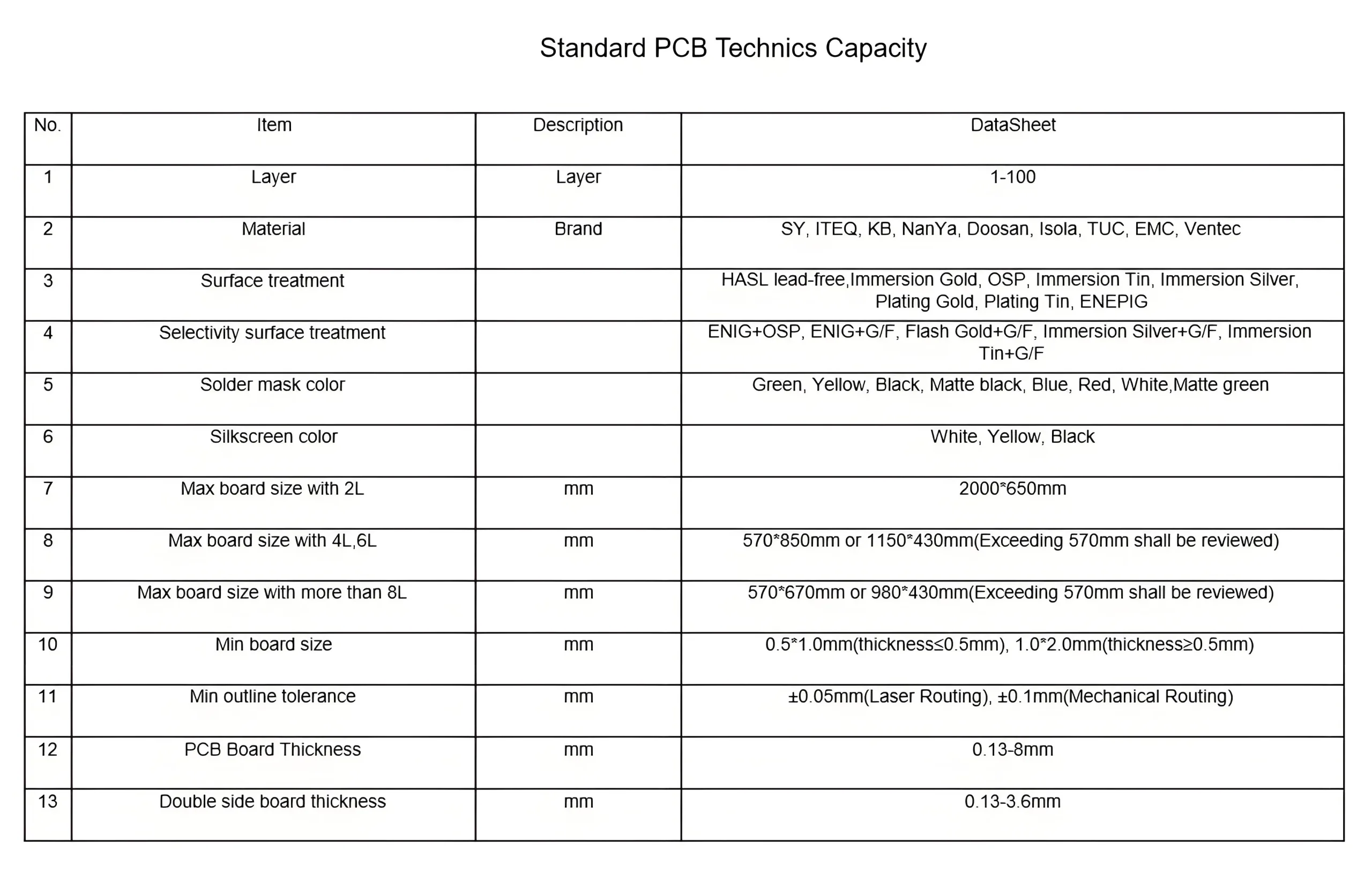
- FR-4 등급 A 재료를 사용하여 최대 100층 PCB 제조
- Precision lamination with ±15um layer-to-layer alignment
- 박리를 방지하는 온도/압력/시간 제어 공정
- 높은 Tg 물질을 위한 옵션, 고속 라미네이트, 최대 1000μm의 무거운 구리
솔더 마스크 & 표면 마감 옵션
- 솔더 마스크 색상: 최소 0.08mm 솔더 브리지가 있는 녹색/파란색/빨간색/검은색
- 표면 마감:
- HASL (열기 솔더 레벨링)
- 동의하다 (무전해 니켈 침지 금)
- 침수 주석/은
- OSP (유기 용해성 보존)
종합적인 QC & 테스트 시스템
- AOI 검사: 라인/스페이스에 대한 고해상도 결함 감지, 패드, 반바지/오픈
- 임피던스 제어: 고속/RF 애플리케이션에 대한 허용 오차는 ±10%입니다.
- 전기 테스트: 플라잉 프로브 & 설비 기반 연속성 검증
- 신뢰성 테스트: 열 충격, 내습성, 굴곡 테스트
공정능력 & 안정
- CPK >1.33 (4에이) 중요한 프로세스 전반에 걸쳐, 도달하다 1.67 (5에이) 주요 분야에서
- ±15% 이내의 선폭 제어 (대 산업 20% 기준)
- 통계적 공정 관리 (SPC) 일관된 생산 품질 보장
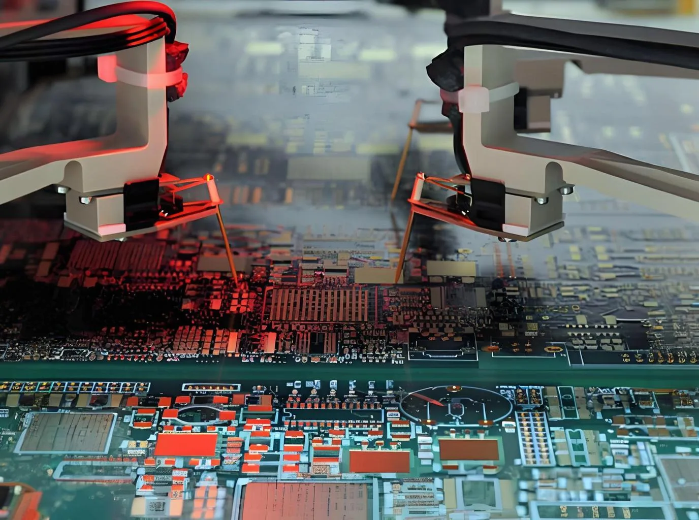
PCBA 원스톱 서비스
- SMT 어셈블리: 01005 ±0.03mm 배치 정확도로 부품 처리
- 고급 포장: X-Ray 검사를 통한 BGA/Micro BGA/PoP 지원
- DFM 지원: 임피던스 계산, 스택업 디자인, 제조 가능성 분석
산업 응용 & 연락하다
가전제품 서비스, 산업 제어, 통신, 의료기기, 맞춤형 PCB 솔루션을 갖춘 자동차 부문. 프로세스 능력 보고서 및 무료 DFM 상담을 보려면 당사 웹사이트를 방문하세요..
위챗
WeChat으로 QR 코드를 스캔하세요