
마이크로 전자 공학의 생명 또는 죽음 전투: 솔더 마스크 갭-유도 된 연쇄 반응
와 함께 0201 구성 요소와 0.3mm 피치 BGA가 주류가됩니다, PCB 패드 솔더 건너 뛰기 속도 급증했습니다 37% (IPC 2023 데이터). 10 년 동안의 연구에 따르면 UGPCB: 60% SMT 결함의 페이스트 전송 고장에서 비롯됩니다, 어디 마이크로 패드 인쇄 갭 간과 된 사람으로 행동하십시오 “보이지 않는 살인자”.
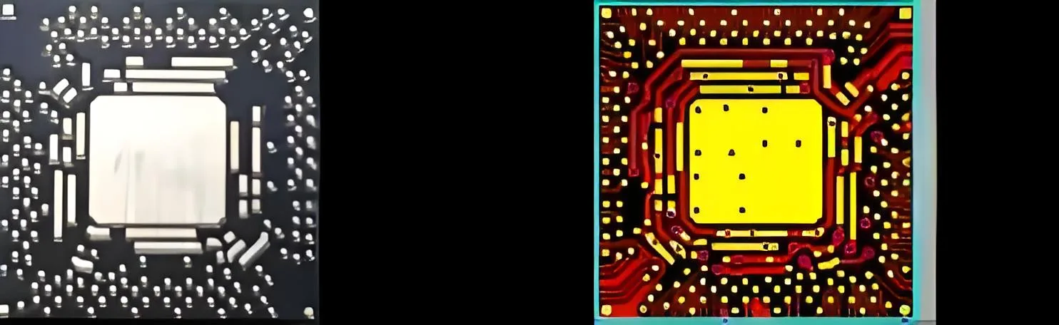
피로 쓰여진 교훈: 현미경 사진은 산업의 진통 점을 보여줍니다
-
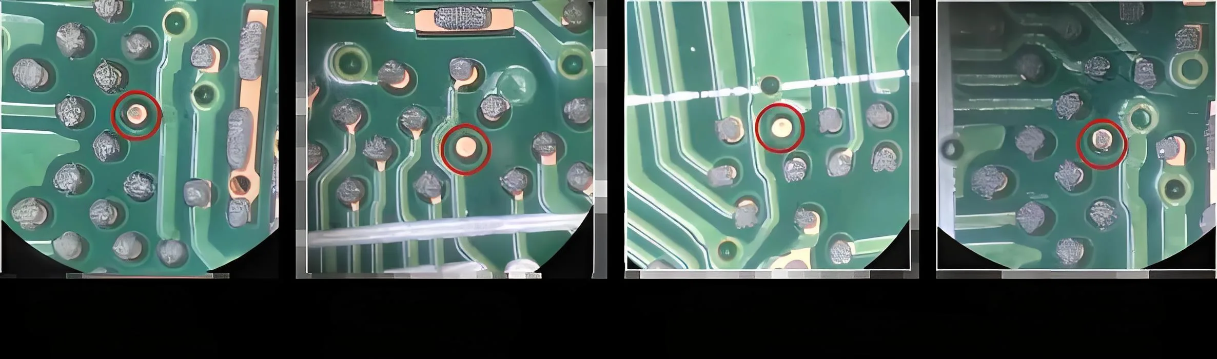
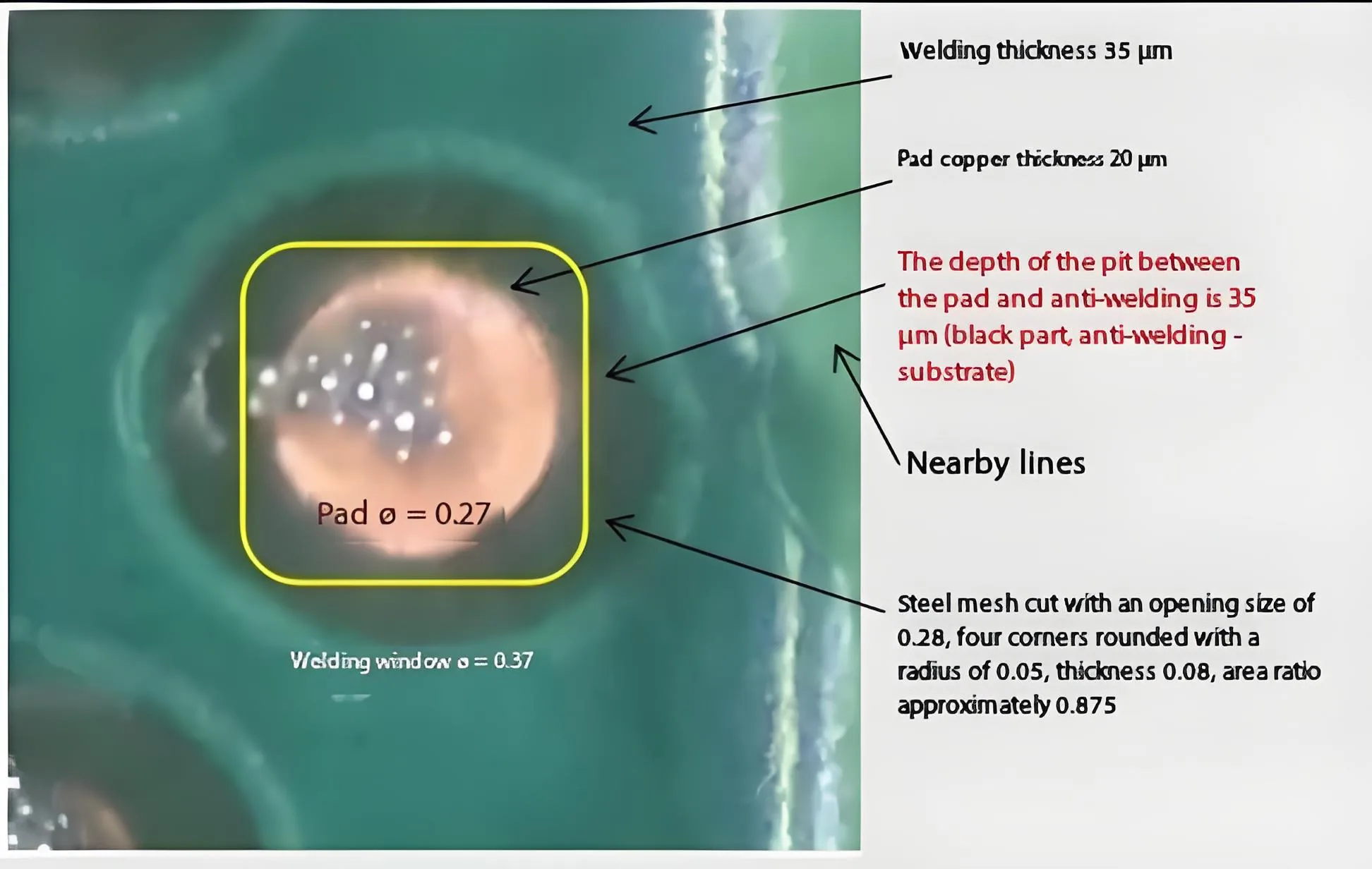
솔더 마스크에서 구리 패드 높이 차이: 35μm
-
기판 영역을 덮는 스텐실 조리개: 42%
-
효과적인 솔더 페이스트 접촉 영역: <58%
실패의 물리학: 수학적 “죽음의 삼각형” 페이스트 전달
치명적인 공식: IPC-7525 면적 비율 이론의 붕괴
면적 비율 = (l × w) / [2시간(l+w)]
PAD 직경 ≤0.3mm 일 때 전통적인 이론이 실패합니다! 주요 제조업체의 경험적 데이터가 나타납니다:
| 패드 직경 (mm) | 이론적 영역 비율 | 실제 전송률 |
|---|---|---|
| 0.40 | 0.68 | 92% |
| 0.31 | 0.61 | 85% |
| 0.27 | 0.55 | 63% |
유체 역학 노출: 왜 땜납 페이스트 “거부합니다” 패드
수치 2: 스텐실 방출 중 유체 장력 시뮬레이션
대체: 솔더 페이스트 스텐실 벽 장력 분석 – PCBA 인쇄 결함 시뮬레이션 – SMT 솔루션
중요한 발견:
-
솔더 마스크 갭은 공기 쿠션 효과를 만듭니다, 접촉 영역 감소 41%
-
솔더 건너 뛰기는 페이스트 응집력이있을 때 발생합니다 > 패드 접착력
산업 등급 솔루션: 솔더 건너 뛰기를 제거하기위한 3 개의 기둥
패드 디자인 혁명: 구리 확장 원리
-
분리 된 패드 직경: 0.27mm → 0.31mm
-
갭 커버리지가 감소했습니다 12%
-
전송률이 증가했습니다 89% (경험적 데이터)
솔더 마스크 “슬리밍” 계획: 25μm 골드 표준
수치 3: 다른 솔더 마스크 두께와의 인쇄
대체: PCB 솔더 마스크 두께 비교 – SMT 수율 개선 – PCBA 공급 업체 안내서
두께 공식: h = (RZ + 디) × k
(δ = 입자 크기를 붙여 넣습니다, 유형 4: 25μm; K = 안전 계수 1.2)
산업 검증: 모바일 PCB 제조업체는 두께를 35μm에서 22μm로 줄였습니다 → 82% QFN 솔더 스킵의 감소
pH 스텐실: 궁극적 인 나노 성분 솔루션
 혁신:
혁신:
-
조리개 디자인: 벽각은 7 ° ~ 15 °입니다
-
전자식 니켈: 3x 경도 증가
-
데 몰딩 보조 각도: 40% 벽 마찰 감소
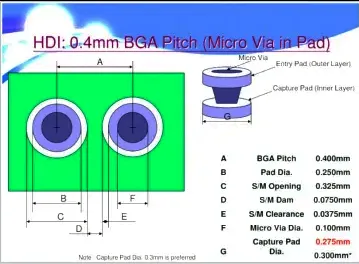
업계 리더’ 플레이 북: HDI + NSMD 골드 표준
모바일 산업의 정밀 전략
사례: 0.4MM 피치 BGA 프로세스 청사진
1. 전설 인쇄 → 베어 구리 설계를 교체하십시오
2. 구현하다 HDI 마이크로 비아
3. 솔더 마스크 두께: 18± 3μm (IPC-6012 클래스 3 준수)
변환 엔진: 공장 업그레이드 행동 계획
즉시 실행 점검표:
-
모든 고립 된 패드를 감사합니다: 직경이 재 설계됩니다 <0.3mm
-
솔더 마스크 두께 보고서를 요구합니다 PCB 공급 업체 (주요 메트릭: ≤25μm)
-
PH 스텐실을 시급히 조달하십시오: 55% 미세 피치 영역에서 조리개 효율이 증가합니다
