
소개
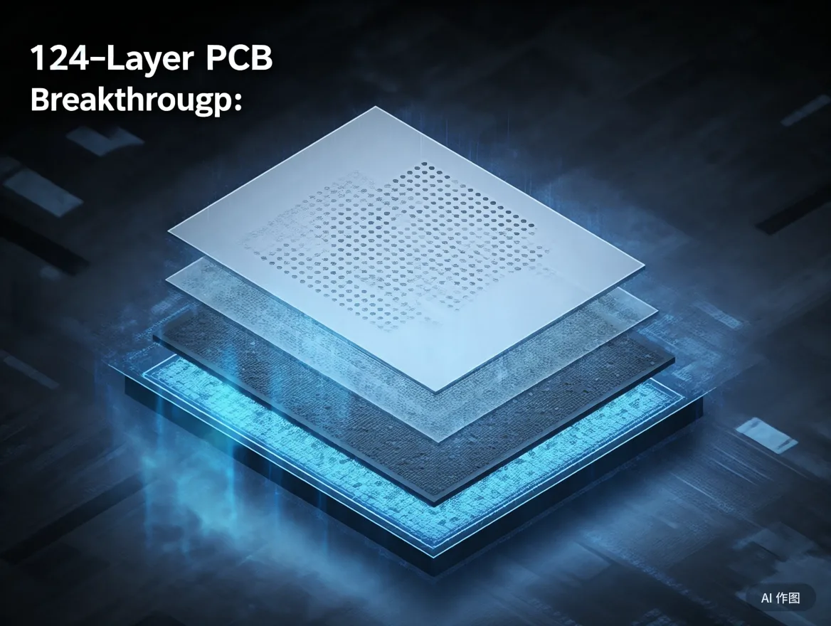
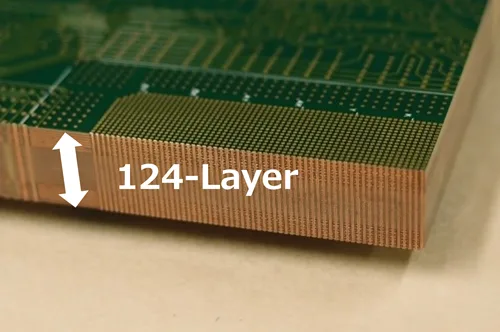
인공 지능에 의해 구동됩니다 (일체 포함) 고성능 컴퓨팅 (HPC), 글로벌 전자 산업은 “고밀도, 고속, 높은 신뢰성.” 5월 2025, 선도 PCB 제조업체 세계 최초의 상업용 124 계층 인쇄 회로 보드를 공개했습니다, 표준 7.6mm 보드 두께를 유지하면서 오랫동안 108 층 산업 장벽을 깨기. 이 이정표는 AI 서버에 대한 중요한 하드웨어 지원을 제공 할뿐만 아니라, 반도체 테스트, 그리고 방어 시스템이지만 전자 포장 기술의 새로운 국경을 잠금 해제합니다..
108 층 장벽을 깨뜨립니다: 124 층 PCB 뒤에있는 엔지니어링 솔루션
정밀 제조 혁신
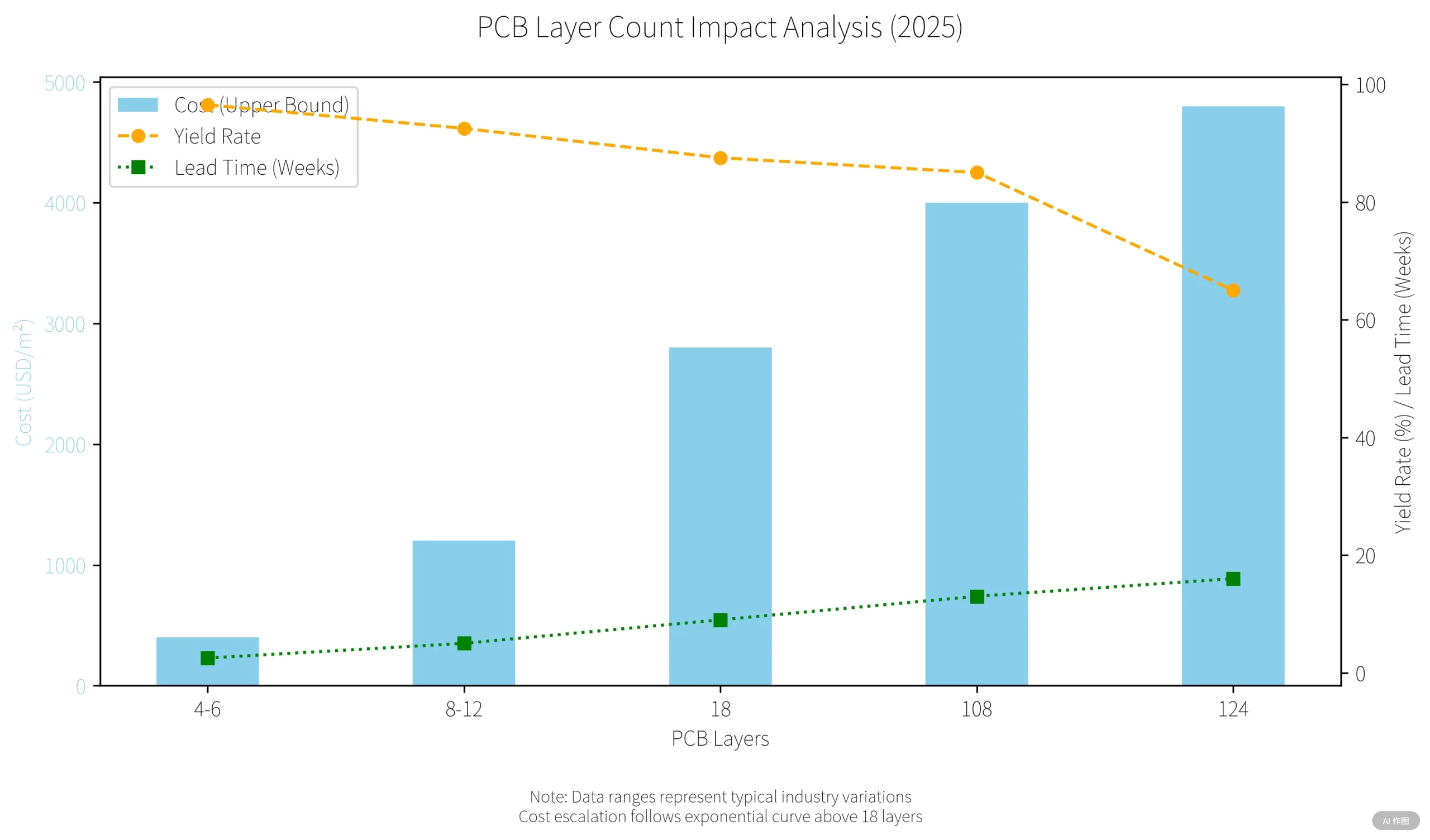
전통적인 PCB 디자인 기계적 및 열 제한에 직면합니다 100 수지 흐름 불일치로 인한 층, 붕괴를 통해, 그리고 계층 오정렬. 획기적인 124 층 PCB는 a 15% 층이 증가합니다:
-
울트라 얇은 유전체: 25저 손실 재료를 사용한 µm 층 (예를 들어, 쓰러뜨리다 7) ± 5% 임피던스 제어 112+ GHZ 신호
-
3D 상호 연결 최적화: 0.15mm²/mm 신호 밀도를 활성화하는 Microvia 어레이, PCIE Gen6 및 CXL을 준수합니다 3.0 프로토콜
열 신뢰성 인증
MIL-STD-883G 표준에 따라 인증, 124 층 PCB가 견딜 수 있습니다 1,000+ 열주기 (-55° C ~ 125 ° C) 유지하는 동안 <1% 신호 손실 80 MPA 기계적 스트레스 - 항공 우주 및 방어 적용에 이상적.
응용: AI 하드웨어 및 반도체 발전 가속화
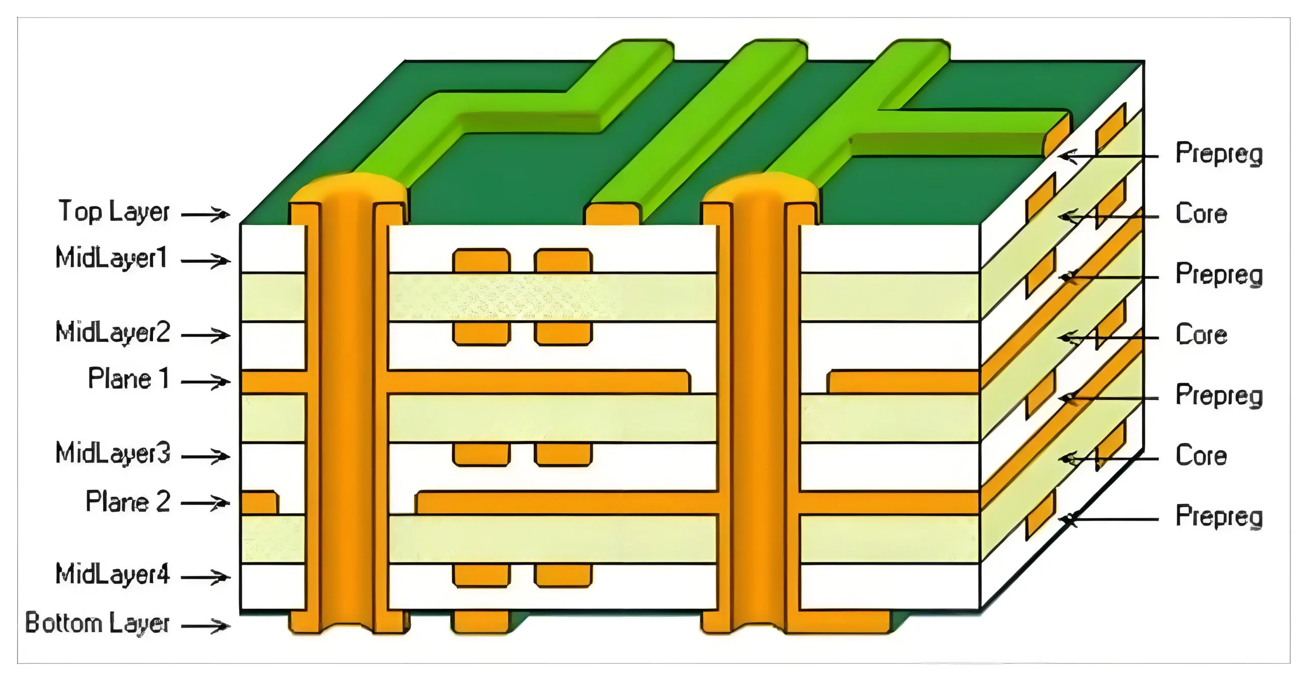
AI 서버 & 대역폭 메모리 (HBM)
-
신호 밀도: 18% 레이어 당 차동 쌍 라우팅의 증가
-
열 관리: 구리로 채워진 마이크로 비아는 열전도율을 향상시킵니다 30%, 500W+ AI 가속기에 중요합니다
웨이퍼 수준 테스트 & 3D 포장
하위 마이크론 정렬 정확도를 활성화합니다 (± 0.8mm) 스택 된 HBM 모듈의 피코 초 수준 신호 지연 제어-칩 렛 기반 아키텍처를위한 게임 체인저.
비용 문제 & 확장 성 로드맵
제조 경제학
-
재료 비용: 4,800/M2(대.3,200/108 층의 경우 m²)
-
수율 요율: 65% (16-주주기) 대. 85% 기존의 경우 HDI
-
실패 분석: 파괴적인 단면화가 필요합니다 20% 열 응력 결함
산업 채택 경로
-
첨가제 제조: 라미네이션 단계를 줄입니다 40%
-
AI 중심 EDA: 스트레스 지점을 통해 예측합니다 92% 정확성, 잠재적으로 수익성을 높일 수 있습니다 75%
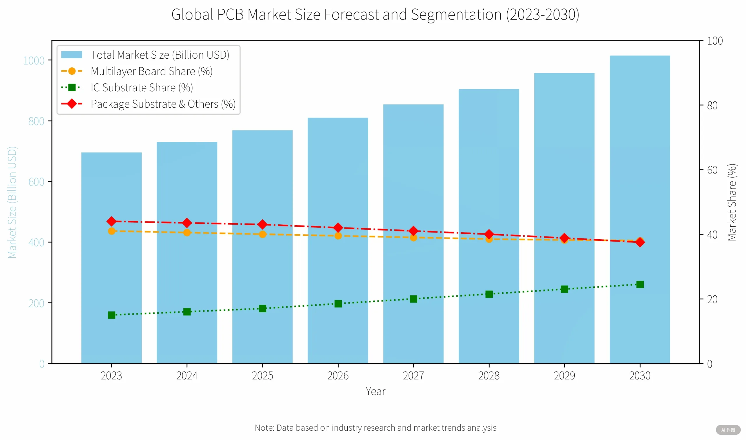
시장 전망: $49B PCB 산업 혁신
성장 동인
-
클라우드 컴퓨팅: 70% AI 서버 PCB의 CAGR (CITIC 증권 2026 투사)
-
에지 AI 장치: 30% 차세대 스마트 폰의 PCB 비용 증가 (애플의 공급망 데이터)
-
현지화 트렌드: 중국 제조업체는 좋아합니다 UGPCB 고급 기판의 3.6m m²/년 용량을 목표로합니다
결론: 계층 수 레코드에 대한 실질적인 혁신
Denso의 129 층 프로토 타입을 능가하지는 않습니다 (2012), 이 124 층 PCB는 새로운 상업 벤치 마크를 설정합니다:
-
표준화 된 두께 (7.6mm) 후진 호환성
-
MIL-SPEC 신뢰성 85% 프로토 타입 비용
-
확장 가능한 제조 공정
양자 컴퓨팅 및 6G가 등장합니다, PCB 혁신은 레이어 수보다 기능 밀도를 우선시합니다. 지속 가능한 기술 진보를위한 중요한 변화.
