
소개: 폭풍의 눈의 기초
반도체 산업의 스포트라이트 아래, 그만큼 인쇄 회로 기판 (PCB) 오랫동안 침묵의 역할을 해왔습니다., 기초 기둥. 하지만, ~에 2025, 원자재 가격 폭풍, 금과 구리를 입힌 라미네이트가 이끄는 (CCL), 공급망 비용 압박의 최전선에 PCB를 밀어 넣었습니다.. 이번 폭풍은 우연이 아니다; AI 인프라 확장으로 인한 기하급수적인 수요 증가와 제한된 공급 능력 사이의 격렬한 충돌입니다.. 이 기사에서는 PCB 산업의 비용 문제와 기본 동인에 대한 전문적인 분석을 제공합니다., 위기 속에서 얼마나 심오한 기술 변화가 가치 도약을 가능하게 하는지 밝혀드립니다.. 신뢰성을 추구하는 기업에 중요한 통찰력을 제공합니다. PCB 공급 업체 그리고 고품질 PCB 서비스.
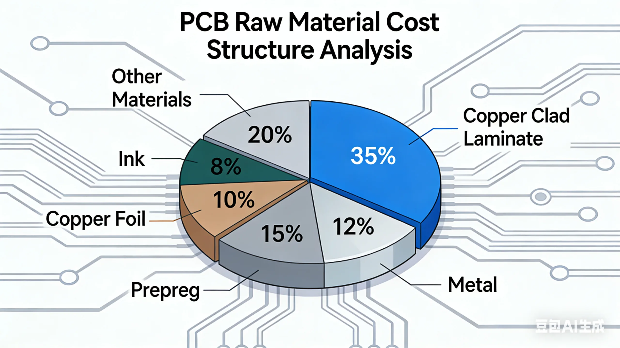
나. 비용 분해: 그만큼 “금과 은” 낙타의 등을 부러뜨리는 빨대
A의 원자재 비용 구조 PCB 복잡하다, 그러나 금과 구리를 입힌 라미네이트는 의심할 여지 없이 가장 무거운 두 가지 재료입니다. “가중주.” 업계 권위 있는 기업 프리즈마크(Prismark)의 분석에 따르면, 일반적인 다층에서 서버용 PCB, CCL은 다음을 설명할 수 있습니다. 30%-40% 비용의, 금과 같은 귀금속은 도금 및 표면 마감에 사용됩니다. (예를 들어, 동의하다) 설명할 수 있다 8%-15%. 함께, 전체 자재비의 절반에 육박합니다.. 이는 다음과 같이 단순화될 수 있습니다.:
PCB 원료 비용 ≈ (CCL 비용 × 공유) + (귀금속 비용 × 점유율) + (기타 재료비)
(원천: 프리즈마크 Q3 2025 PCB 재료 비용 분석 보고서)
1. 금: 반짝이는 마감 그 이상
고급스러운 골드 PCB 우수한 전도성을 보장하기 위해 중요한 연결부의 표면 마감에 주로 사용됩니다., 내산화성, 및 납땜성. 시안화금칼륨의 가격 (금염), 예를 들어, 업계의 지표가 되었습니다. 한국의 주요 데이터 PCB 제조업체 놀라운 궤적을 보여줍니다: 대략적으로 50,000 원/그램 단위 2023 에게 99,000 2025년 3분기 원/그램 - 거의 100% 증가하다. 이는 제조 비용을 직접적으로 증가시킵니다. HDI PCB ENIG와 같은 프로세스를 사용하는 IC 기판 (무전해 니켈 침지 금). 대용량이 필요한 고객의 경우 PCBA 조립, 이 비용 이전은 중요합니다.
2. 동박 적층판: AI 수요의 직접적인 통로
회로 패턴을 운반하는 핵심 유전체로서, CCL의 성능이 최종 결정을 직접적으로 결정합니다. PCB 신호 무결성, 열 관리, 신뢰성. AI 서버, 고속 스위치, 그리고 AI 가속기 카드 데이터 처리량 및 신호 손실에 대해 거의 까다로운 요구 사항을 부과합니다., 고속/고주파 수요 폭발적 증가, 초저손실 (예를 들어, 초저손실, 매우 낮은 손실 등급) 라미네이트.
삼성전기 등 일류 제조업체의 피드백 - 10%-15% 3분기 전년 대비 조달 비용 증가 - 이러한 구조적 공급 긴장을 잘 보여줍니다.. 이는 특히 다음 분야에 사용되는 고성능 라미네이트의 경우에 해당됩니다. AI 서버 마더보드 그리고 GPU 가속기 카드 PCB.
II. 뿌리 깊은 운전자: PCB 수요 지도를 재편하는 AI 열풍
원자재 비용 상승은 표면적인 증상입니다.; 핵심 엔진은 글로벌 디지털 및 지능형 혁신입니다, 특히 AI 컴퓨팅 인프라의 군비 경쟁.
1. 역할 진화: 에서 “커넥터” 에게 “시스템에 중요한 구성 요소”
전통적으로, PCB 구성 요소에 대한 기계적 지지대 및 전기 연결 플랫폼으로 간주되었습니다.. AI 시대에는, 이 역할은 근본적으로 바뀌었습니다. 차세대 아키텍처, NVIDIA의 Rubin과 같은 플랫폼이 그 예입니다., 매우 높은 내부 상호 연결 대역폭과 밀도 추구, 높은 레이어 카운트 만들기 PCB (일반적으로 22+ 레이어) 그리고 모든 계층 HDI 기술 표준. 모든 흔적은 PCB 데이터 대기 시간 및 전력 소비에 영향을 미칩니다.; 설계 및 제조 정밀도는 CPU/GPU 간의 시너지 효율성에 직접적인 영향을 미칩니다., 메모리, 그리고 가속기. 업계 분석에 따르면 AI 서버 마더보드 값은 표준 서버의 몇 배입니다., 그것으로 PCB 부분 그에 따른 기술 콘텐츠 및 가격의 증가 확인.
2. 기하급수적인 수요 증가 사양
AI 훈련 및 추론은 구체적이고 엄격한 결과를 생성합니다. PCB 요구 사항:
-
증가된 레이어 수: 더 복잡한 전력 공급 네트워크와 더 많은 신호 계층을 수용하기 위해, AI 서버 마더보드 레이어 수가 점점 늘어나고 있습니다. 30 레이어와 그 이상.
-
재료 업그레이드: 224Gbps 이상으로 이동하는 데이터 속도로 인해 M6에 대한 수요가 증가하고 있습니다., M7급 초저손실 라미네이트 (Df만큼 낮음 0.0015).
-
크기 & 완성: 더 많은 컴퓨팅 유닛을 통합하기 위한 더 큰 보드 크기, 임베디드 구성 요소와 같은 고급 프로세스 PCB 통합 및 성능 향상.
에 따르면 IPC (전자산업을 연결하는 협회) 2025 전망 보고서, 글로벌 하이엔드 PCB 시장 데이터 센터 및 AI 인프라의 CAGR은 14% ~에서 2024 에게 2028, 업계 평균을 훨씬 웃도는.
III. 가치 도약: 기술 혁신을 통한 앞으로의 길
깃 달기 “분쇄 비용,” 주요한 PCB 제조업체 수동적으로 버티지 않고 적극적으로 기술고지를 향해 전진하고 있습니다., 제품 가치 변화를 통한 압박 해소 및 신규 시장 개척.
1. 하이엔드 제품 포트폴리오를 향한 전략적 전환
“고부가가치 제품을 통한 수익성 추구” 업계 합의다. 주요 경로는 다음과 같습니다:
-
고급 패키징 기판에 중점: Chiplet과 이기종 통합이 트렌드가 되면서, FC-BGA용 기판 수요 (플립칩 볼 그리드 어레이) 포장이 급증하고 있다. 이 기판은 매우 미세한 선 폭/간격을 특징으로 합니다. (10μm/10μm 이하까지), 기술적인 장벽이 높다, 더 큰 이익 마진을 제공합니다..
-
차세대 메모리 인터페이스에 투자하세요: 1c나노미터 공정 기반 DRAM, 주변의 상용화를 목표로 2026, 에 대한 수요를 촉진할 것입니다. PCB 8Gbps+에서 DDR5 메모리 인터페이스 지원. 뿐만 아니라, SoCAMM PCB (압축 부착 메모리 모듈), AI 서버에 특화된 미래 메모리 솔루션, 새로운 성장 포인트를 제시하다 PCB 설계 그리고 제조.
-
ASIC 물결 수용: 사내 AI 칩 (ASIC) Google과 같은 클라우드 거대 기업의, 아마존, Microsoft는 맞춤형 고밀도 상호 연결에 대한 수요를 촉진하고 있습니다. (HDI) ASIC 기판. 고속을 강조하는 제품입니다, 밀도, 신뢰성, 전형적인 고부가가치 항공사를 대표하는 프론트엔드 PCB 프로세스.
2. 혁신을 통한 비용 효율성 최적화
단순히 비용을 전가하는 것은 지속가능하지 않습니다.. 기술 혁신을 통해 비용 효율성을 높이는 것이 핵심 차별화 요소입니다..
-
설계 최적화: 고급 시뮬레이션 도구를 사용하여 레이아웃 설계 최적화, 성능을 보장하면서 잠재적으로 레이어 수를 줄이거나 보다 비용 효율적인 재료 대안을 사용합니다..
-
프로세스 혁신: 재료 활용도를 높이기 위해 제조 공정 개선 (예를 들어, CCL 패널 최적화) 금 두께를 최소한의 신뢰성 있는 기준으로 감소시킵니다. (준수합니다 IPC-4552/4556 명세서).
-
공급망 협업: 성능과 비용의 균형을 맞추는 맞춤형 소재 솔루션을 공동 개발하기 위해 라미네이트 및 화학 공급업체와 전략적 파트너십 구축.
R의 경우&D 기업이 요구하는 PCB 프로토 타이핑 그리고 저용량 PCBA 생산, 이러한 고급 경로에 대한 통합 설계-제조-조립 서비스와 전문 지식을 제공하는 파트너를 선택하는 것이 중요합니다..
IV. 미래의 전망: 2026, PCB 가치 리모델링의 변곡점
2026 2019년은 가치 리모델링의 중추적인 해로 널리 알려져 있습니다. PCB 산업. 한편으로, 새로운 생산 능력이 가동되면서 원자재 비용 압박이 부분적으로 완화될 수 있습니다.. 더 중요한 것은, AI가 주도하는 기술 업그레이드로 인한 배당금, HPC (고성능 컴퓨팅), 그리고 고속통신 (예를 들어, 5.5G/6G) 완전히 드러날 것이다.
측정항목 PCB 가치 에서 진화할 것이다 “평방미터당 가격” 더 향해 “대역폭 단위당 비용” 또는 “와트당 효율성 비용.” PCB 제조업체 신호 무결성에 대한 심층적인 전문 지식을 갖춘 시스템 수준 솔루션 제공 가능, 전력 무결성, 열 관리는 확실한 경쟁 우위를 확보할 것입니다..
결론: 폭풍의 눈에 해자 만들기
무슨 PCB 산업 겪고 있는 것은 “성장통” 강력한 수요와 엄청난 기술 변화에 힘입어. 금과 라미네이트의 가격 변동은 이 거대한 이야기에서 가장 눈에 띄는 장일 뿐입니다.. 핵심 이야기는 이렇습니다 PCB 전자제품 분야의 무대 뒤에서 중앙 무대로 이동하고 있습니다., 고성능 컴퓨팅 시스템의 성능이 직접적으로 결정되는 성능.
전자제품 브랜드 및 R용&D사, 이제는 재평가할 때다 PCB 조달 전략 그리고 PCBA 파트너. 단순한 단가를 넘어서, 다층 기판에 대한 공급업체의 기술 역량 및 대량 생산 경험에 대한 심층 평가, 고속 재료 적용, 고급 패키징 상호 연결이 필수적입니다.. 비용 문제에 대비해 설계를 공동 최적화하기 위해 미래 지향적인 기술 리더와 협력하는 것이 미래 시장에서 승리하는 열쇠가 될 것입니다..
차세대 AI를 위한 맞춤형 회로 솔루션과 정확한 견적을 받으려면 지금 전문 PCB/PCBA 공급업체에 문의하세요., 데이터 센터, 또는 고급 통신 제품, 그리고 이 기술 급증의 주도권을 잡으세요.
