
1. PCB 기술 진화 및 혁신 동인
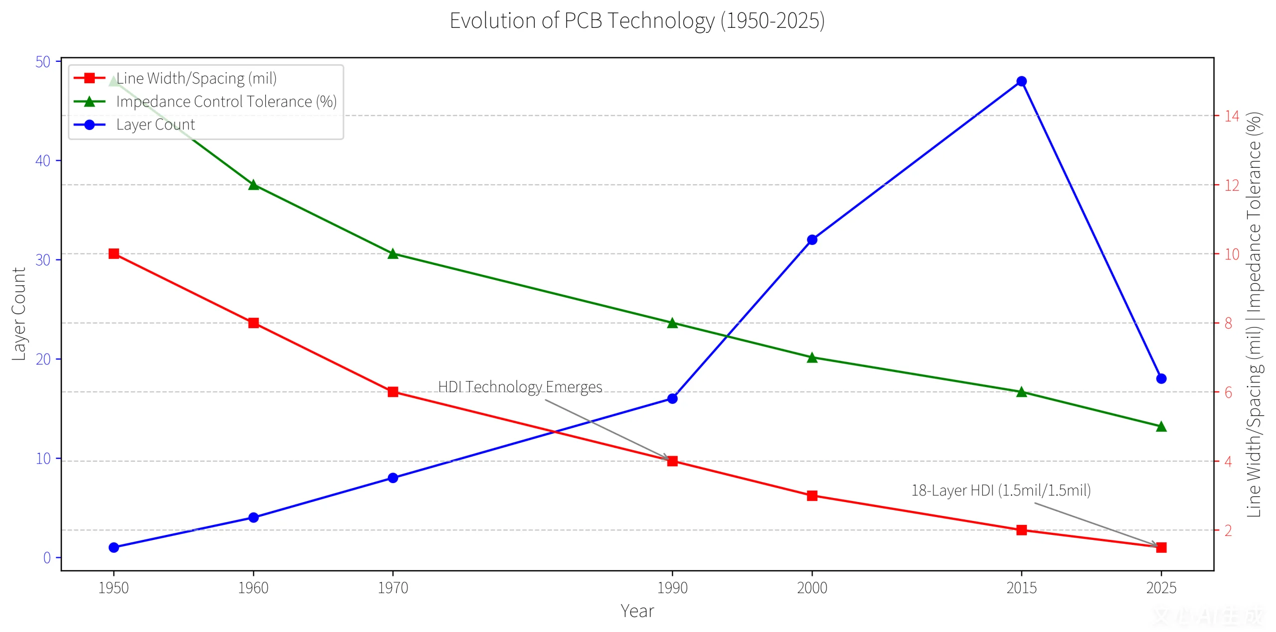
그만큼 PCB (인쇄 회로 기판) 역할을합니다 “전자 제품의 어머니,” 구리 트레이스 및 패드를 통한 구성 요소의 기계적 고정 및 전기 연결 활성화. 최신 PCB는 단일 층 보드에서 고밀도 상호 연결로 진화했습니다. (HDI) 다층 보드, 고성능에 대한 요구에 의해 주도됩니다, 소형화, 신뢰성.
주요 시장 동인:
- AI 서버 요구가 급증했습니다 60% 요 2025, HDI 강화 및 다층 PCB 양자.
- 자동차 전자 공급, 특히 EV에서, 고출성 PCB 성장을 연료로 연료.
- UGPCB의 10 층 1 차 PCB는 신호 손실을 줄입니다 42% 2mil 트레이스 및 레이저 미세 연소 기술 사용.
기술 혁신:
- 1.5mil/1.5mil의 추적 폭/간격 (업계 평균: 3밀).
- ± 5%의 임피던스 제어 공차 (업계 표준을 초과합니다 10%).
2. PCB 분류 및 응용 프로그램
2.1 레이어 기반 분류
단일 계층 PCB: 간단한 디자인 (예를 들어, 장난감, 전원 어댑터).
더블 레이어 PCB: 상호 연결을 위해 VIA를 사용합니다; 라우터 및 홈 가전 제품에 이상적입니다.
다층 PCB (3+ 레이어): 스마트 폰을위한 고밀도 설계, 자동차 시스템, 및 산업 컨트롤러.
2.2 재료 & 프로세스 기반 분류
견고한 PCB: 고정 형식 장치의 FR-4 기판 (전화, TV).
유연한 PCB (FPC): 구부릴 수있는 응용을위한 폴리이 미드 기반 (스크린 케이블, 웨어러블).
RIDID-FLEX PCB: 복잡한 어셈블리를 위해 단단하고 유연한 섹션을 결합합니다 (드론, 의료기기).
3. 응용 프로그램 별 요구 사항
3.1 가전제품
- 스마트폰: 12-CPU 용 층 강성 PCB, 카메라, 및 RF 모듈.
- 노트북: 6-10 CPU 용 레이어 보드; 배터리 연결 용 FPC.
3.2 산업 전자 제품
- PLC 컨트롤러: 4-6 모터 제어를위한 EMC 저항이있는 층 PCB.
- 센서: 가혹한 환경에서 안정적인 신호 전송이있는 이중층 보드.
3.3 자동차 전자
- EV 배터리 관리: 전압/온도 모니터링 용 다층 PCB.
- ADAS 시스템: 밀리 초 레벨 응답이있는 고출력 보드.
3.4 고급 응용 프로그램
- 5G 기지국: 8-12 고주파 신호 무결성을위한 RF 보드.
- 의료 기기: ECG 기계를위한 생체 적합성 재료를 갖춘 다층 PCB.
4. 시장 데이터 및 성장 예측
- 글로벌 PCB 시장: 155.38b by 2037.
- HDI 보드: 33.4% 시장 점유율 2037, 스마트 폰 및 AI 서버로 구동됩니다.
- 자동차 PCB: 18.79b by 2035 (cagr 5.5%).
중국의 지배: 계정 50% 글로벌 생산의; 고급 PCB에 도달합니다 40% 공유하십시오 2025.
5. PCB 및 SMT 시너지
PCB 디자인 및 SMT (표면 실장 기술) 상호 의존적입니다:
- PCB는 SMT 구성 요소를위한 정확한 솔더 패드 레이아웃을 제공합니다 (예를 들어, 0402 저항기: 0.4mm × 0.2mm).
- SMT는 고밀도 어셈블리를 가능하게합니다, 스마트 폰 PCB의 BGA 칩과 같은.
UGPCB의 장점: LPKF 레이저 이미징 시스템은 ± 25μm 정렬 정확도를 달성합니다, HDI 생산에 중요합니다.
6. 미래의 도전과 트렌드
비용 압력:
- 구리 가격 상승 15% ~에 2025;구리 클래드 라미네이트 (CCL) 비용이 상승했습니다 8-12%.
- 중소기업은 마진 압축에 직면합니다, 산업 통합 가속화.
기술 변화:
- 수요 증가 8-16 층 PCB 및 IC 기판 (시장 규모: $45b by 2025).
- 저전력, 친환경 디자인을위한 고층 컨덕션 재료.
글로벌 확장:
- 동남아시아에 투자하는 PCB 제조업체 (베트남, 태국) 비용 효율성 및 관세 회피.
결론
PCB 산업은 글로벌 전자 제품에 중추적 인 상태로 남아 있습니다, AI에 의해 운전됩니다, 자동차, 5G 혁신. 회사는 기술 업그레이드의 우선 순위를 정해야합니다, 공급망 다각화, 비용 변동성과 지역 경쟁에서 번성하기위한 녹색 제조.
