

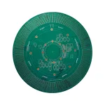
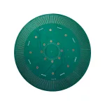
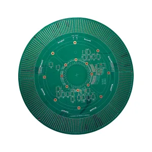
UGPCB의 ATE 프로브 카드 PCB 소개
UGPCB의 50 층을 먹었습니다 (자동 테스트 장비) 프로브 카드 PCB 고주파 반도체 테스트를 위해 설계된 정밀 엔지니어링 솔루션입니다. 테스트 장비와 통합 회로 간의 정확한 신호 전송을 가능하게합니다. (ICS), 미션 크리티컬 환경에서 안정적인 성능을 보장합니다.
주요 기술 사양
-
레이어 수: 50 레이어
-
두께: 198 밀
-
재료: FR4 HTG (고온 유리 에폭시)
-
최소 구멍 크기: 5 밀
-
BGA 간격: 0.35mm
- 구리 두께:2/2온스
-
종횡비: 40:1
-
드릴-카퍼 거리: 3 밀
-
POFV (채워진 위에 도금되었습니다): 예
-
표면 마감: 에그 (전기 전기 니켈 전기 금)
설계 및 구조 혁신
중요한 설계 기능
-
고밀도 상호 연결: 50 층 아키텍처는 0.35mm 피치로 BGA 구성 요소의 초 미세한 라우팅을 지원합니다., 현대 IC 테스트에 필수적입니다.
-
고급 자료: FR4 HTG는 열 안정성을 보장합니다 (TG ≥ 180 ° C), 고출력 테스트주기 동안 변형 방지.
-
정밀 드릴링: 에이 40:1 종횡비 및 5 MIL Microvias는 엄격한 간격 레이아웃에서 신뢰할 수있는 신호 경로를 가능하게합니다..
-
POFV 기술: 채워지고 도금 된 VIAS는 기계적 강도 및 열 소산을 향상시킵니다., 장기간 테스트 작업에 중요합니다.
구조적 장점
-
초-쇼트 드릴-카퍼 거리: 3 MIL 간격은 신호 손실과 크로스 토크를 최소화합니다.
-
Eneg 표면 마감: 프로브 바늘을위한 탁월한 산화 저항과 안정적인 접촉 표면을 제공합니다..
성능 및 기능 응용 프로그램
운영 원리
PCB는 최소한의 대기 시간으로 테스트 프로브와 IC 사이의 전기 신호를 노선합니다.. FR4 HTG 기판은 열 응력 하에서 유전체 일관성을 유지합니다., POFV는 고 진동 환경에서 중단되지 않은 연결을 보장합니다.
핵심 성과 지표
-
열 내구성: 최대 180 ° C의 온도에서 안정적인 성능.
-
신호 무결성: 제어 된 임피던스 (± 8%) 낮은 삽입 손실 (<0.5DB).
-
기계적 내구성: 기간 동안 박리에 저항합니다 10,000+ 테스트 사이클.
1 차 사용 사례
-
반도체 테스트: 로직 칩을 검증합니다, 메모리 모듈, ATE 시스템의 프로세서.
-
항공 우주 전자 장치: 매우 신뢰할 수있는 PCB가 필요한 항공 전환 테스트 장비에 사용됩니다.
-
5G 및 IoT 장치 생산: 고주파 RF 구성 요소 테스트에서 신호 정확도를 보장합니다.
-
자동차 IC 검증: ADAS 및 ECU 테스트 워크 플로에 배포되었습니다.
생산 프로세스 및 품질 보증
제조 워크 플로
-
재료 절단: FR4 HTG 라미네이트는 필요한 치수에 정밀하게 자릅니다.
-
레이저 드릴링: 달성 5 a 40:1 Co₂ 레이저를 사용한 종횡비.
-
도금 및 충전을 통해: POFV 기술은 구리 도금으로 VIA를 강화합니다.
-
층 정렬: 50-층 스택 업은 고압 및 온도 하에서 결합됩니다.
-
표면 처리: ENEG 코팅은 부식 저항에 적용됩니다.
-
엄격한 테스트: 전기 연속성 검사를 포함합니다, 임피던스 테스트, 및 열 사이클링 검증.
품질 표준
-
IPC-6012 클래스 3 규정 준수: 가혹한 산업 응용 분야의 신뢰성을 보장합니다.
-
100% 자동 광학 검사 (AOI): 고밀도 레이아웃의 미세 감지를 감지합니다.
경쟁력있는 장점 요약
-
매우 높은 밀도: 0.35mm BGA 간격으로 소형화 된 IC 테스트를 지원합니다.
-
열 탄력성: FR4 HTG는 극한 조건에서 안정성을 보장합니다.
-
업계 최고의 정밀도: 5 mil microvias 및 3 MIL 드릴 투 쿠퍼 간격.
-
광범위한 호환성: Teradyne 및 Advantest와 같은 주요 ATE 플랫폼과 호환됩니다.
이 PCB는 최첨단 엔지니어링을 결합합니다, 엄격한 품질 관리, 차세대 반도체 테스트의 요구를 충족하기위한 특수 재료.


