
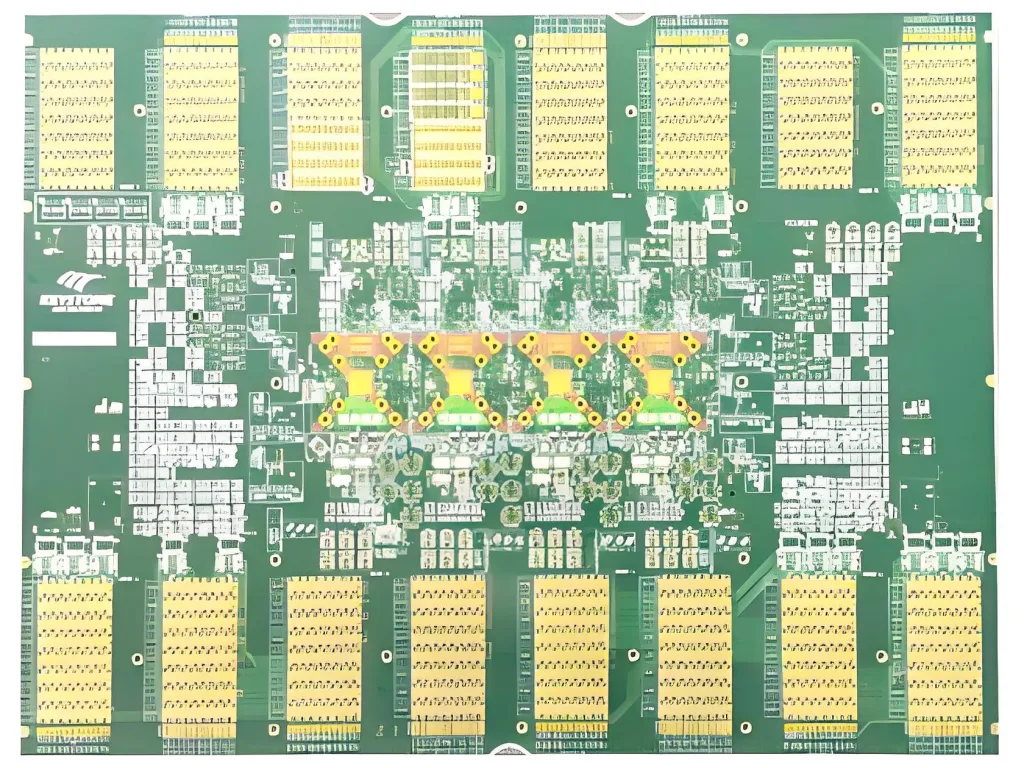
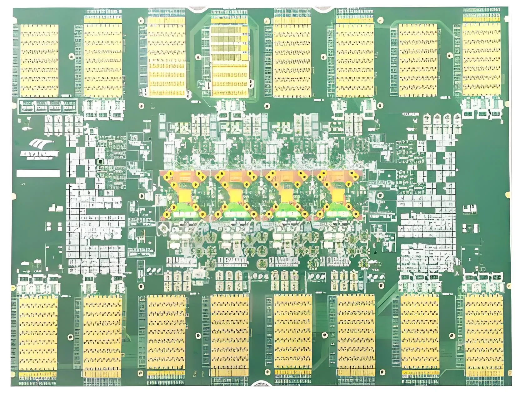
62 층 ATE로드 PCB의 개요
62 층 ATE 부하 PCB는 고성능입니다, 매우 높은 밀도 인쇄 회로 기판 자동 테스트 장비를 위해 설계되었습니다 (먹었다) 시스템. 복잡한 신호 라우팅 및 고전력 부하를 처리하도록 설계되었습니다, 반도체 제조 및 고급 전자 유효성 검사에서 엄격한 테스트 요구 사항을 충족합니다..
핵심 정의
ATE 부하 PCB는 a입니다 특수 회로 보드 통합 회로 테스트를위한 실제 작동 조건을 시뮬레이션합니다 (ICS) 그리고 전자 구성 요소. 62 계층 구성은 복잡한 신호 경로를 지원합니다, 전력 분배, 소형 설계의 열 관리.
중요한 설계 매개 변수
-
레이어 수: 62 다중 도메인 신호 분리 및 전력 평면 최적화를위한 층.
-
치수: 16.9″ × 22.9″ (다중 장치 통합을위한 대형 형식).
-
두께: 250 밀 (강성 및 열 소산의 균형을 유지합니다).
-
재료: FR4 HTG (최대 180 ° C의 안정성을위한 고온 유리 에폭시).
-
최소 구멍 크기: 8 밀 (고밀도 상호 연결을 지원합니다).
-
BGA 피치: 0.65mm (미세 피치 구성 요소 장착을 활성화합니다).
-
종횡비: 32:1 (Microvias에서 안정적인 도금을 보장합니다).
-
드릴-코퍼: 7 밀 (단락을 방지합니다).
-
POFV & 백 링: 고주파 응용 분야에서 신호 왜곡을 제거합니다.
-
표면 마감: 에그 (전기 니켈 전기 금은 부식성을위한 전기 금).
핵심 기능
그만큼 PCB 테스트중인 ATE 시스템과 장치 간의 경로 테스트 신호 (가져왔다), 정확한 전압/전류 측정 보장. 백 드릴링은 신호 반사를 최소화하기 위해 스터브를 통해 사용되지 않은 것을 제거합니다, POFV 동안 (채워진 vias 위에 도금되었습니다) 열전도율과 구조적 무결성을 향상시킵니다.
기본 응용 프로그램
-
반도체 테스트: IC를 확인합니다, CPU, 및 메모리 모듈.
-
항공우주 & 방어: 미션 크리티컬 항공 전자 및 레이더 시스템.
-
통신 인프라: 고속 데이터 전송 장비.
-
의료 기기: 정밀 진단 및 이미징 도구.
물질적 이점
FR4 HTG가 제공합니다:
-
열 탄력성: 순환 열 응력 하에서 안정적인 성능.
-
낮은 유전체 손실: 고주파 신호 무결성에 중요합니다.
-
기계적 강도: 다층 라미네이션 중에 뒤틀림에 저항합니다.
구조적 특징
-
하이브리드 스택 업: 고속을 결합합니다, 힘, 그리고지면 층.
-
마이크로 비아 기술: 레이저-실행 마이크로 비비 아 (8 밀) 밀도가 높은 인터레이어 연결을 활성화하십시오.
-
제어 된 임피던스 추적: 0.65mm BGA 레이아웃에서 Crosstalk를 최소화합니다.
성능 하이라이트
-
신호 무결성: <3% 삽입 손실 10 GHz.
-
파워 취급: 파워 평면 당 20A를 지원합니다.
-
열 관리: 1.2 POFV를 통한 MK 열전도율.
제조 워크 플로
-
재료 준비: FR4 HTG 코어 및 Prepreg 시트를 자릅니다.
-
레이저 드릴링: ± 1 mil 내성으로 8-mil microvias를 만듭니다.
-
도금 & POFV: vias를 전기 배치하고 전도성 에폭시로 채 웁니다.
-
백 링: 깊이 제어 드릴을 사용하여 스터브를 통해 초과를 제거하십시오.
-
라미네이션: 누르다 62 고온/압력 하의 층.
-
표면 마감: 용해성 및 산화 저항성을 위해 ENEG를 적용하십시오.
-
테스트: 임피던스를 검증하십시오, 연속성, 열 순환.
이상적인 사용 사례
-
고주파수 ATE 시스템: 5G RF 구성 요소 및 밀리미터 파 장치를 테스트합니다.
-
다중 사이트 테스트: 병렬 검증 16+ 단일 보드의 DUT.
-
가혹한 환경: 석유/가스 탐사 센서 및 자동차 ECU 테스트.


