
UGPCB: 첨단 반도체 패키징을 위한 고밀도 블라인드 비아 IC 기판
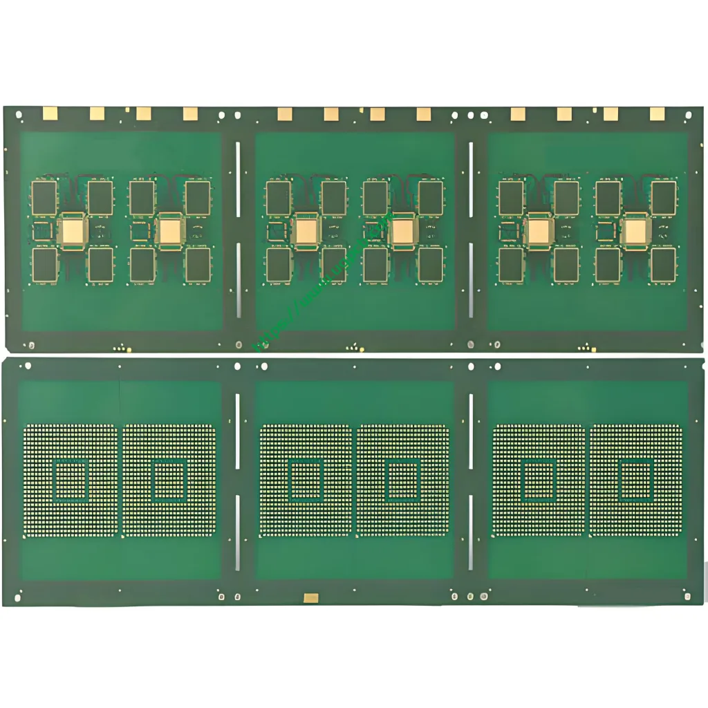
UGPCB의 8층 블라인드 비아 IC 기판, Mitsubishi Gas HF HL832NX 소재로 제작, 차세대 칩을 위한 우수한 신호 무결성과 고밀도 상호 연결을 가능하게 합니다., 30μm 선폭과 0.1mm 마이크로 비아가 특징.
전자제품이 빠르게 발전함에 따라 소형화, 더 높은 밀도, 향상된 성능, 전통적인 스루홀 비아 기술은 현대 칩 패키징의 요구 사항을 충족하기 위해 고군분투하고 있습니다.. 블라인드 비아 기술 위한 중요한 솔루션으로 떠오르고 있습니다. 고밀도 상호 연결 (HDI) 설계.
블라인드 비아(Blind Via)는 전도성 구멍입니다. PCB의 외부 레이어를 하나 이상의 내부 레이어에 연결합니다. 보드 전체를 거치지 않고. UGPCB의 8층 블라인드 비아 IC 기판, 활용 미쓰비시 가스 HF 소재, 이 고급 기술을 예시합니다., 정밀도를 제공, 안정적인 상호 연결 플랫폼 고급 반도체 패키징.
핵심제품: 블라인드 비아 IC 기판에 대해 자세히 살펴보기
Blind Via 기술은 특정 유형의 상호 연결 구조를 정의합니다. 외부 레이어를 인접한 내부 레이어에만 연결합니다.. 스루홀 비아와 달리, 블라인드 비아는 보드 표면에서 시작하여 특정 내부 구리층에서 정확하게 종료됩니다..
이 구조 사용 가능한 배선 공간을 극대화합니다. 불필요한 관통 구멍을 제거하여, 회로 밀도가 크게 증가합니다. 이는 업계의 추진 방향과 완벽하게 일치합니다. 더 작은 폼 팩터와 더 큰 통합.
기술 구현 관점에서, 블라인드 비아의 설계 및 제작은 엄격한 표준을 준수합니다., 에 설명된 것과 같은 IPC-6012 Rigid에 대한 자격 및 성능 사양 PCB. 그들은 일반적으로 다음을 사용하여 형성됩니다. 레이저 드릴링 공정, 테이퍼 구멍 구조 생성. 이를 통해 깊이와 직경을 정밀하게 제어할 수 있습니다., 마이크로 기능 및 정합 정확성을 위한 고급 패키징의 엄격한 요구 사항을 충족합니다..
기술 사양 & 디자인 장점
UGPCB의 Blind Vias IC 기판 디자인은 다음과 같습니다. 고도로 전문화된, 재료 선택부터 스택업 아키텍처까지 중요한 고려 사항이 포함됩니다..
주요 기술 매개변수:
-
모델: 블라인드 비아 IC 기판
-
핵심 자료: 미쓰비시가스HF (HL832NX) BT 에폭시
-
레이어 수: 8 레이어
-
전체 두께: 0.6 mm
-
보드 크기: 40 mm x 55 mm
-
솔더 마스크: PSR-4000 AUS308
-
표면 마감: 부드러운 (무전해 니켈 침지) 금
-
최소 레이저 드릴링 비아 직경: 0.1 mm
-
최소 선 너비 / 공간: 30 μm / 30 μm
이 기판은 일본의 미츠비시 가스 화학 HF 시리즈 BT 재료 (HL832NX), 우수하다고 알려진 유전체 특성 (Dk/Df) 그리고 열 안정성, 고주파수 및 고속 애플리케이션에 이상적입니다.. 그만큼 30μm 미세라인 기술 핀 수가 많은 칩을 연결하는 데 중요합니다., 동안 ENIG 표면 마감 아파트를 제공합니다, 와이어 본딩 가능, 안정적인 납땜 표면.
작동 방식: 정밀한 상호 연결 & 신호 무결성
Blind Vias IC 기판의 핵심 기능은 효율적인 확립, 안정적인 층간 전기 연결 부동산 소비를 최소화하면서 현대적인 포장 요구 사항을 직접적으로 해결합니다. 고밀도 및 우수한 성능.
신호 전송용, 블라인드 비아는 스루홀 비아에 비해 뚜렷한 이점을 제공합니다.. 관통 구멍으로 인해 원하지 않는 결과가 발생할 수 있습니다. 스텁 안테나 역할을 하는 것, 고주파수에서 신호 무결성 저하. 블라인드 비아, 필요한 레이어만 연결, 이러한 비기능적 스텁을 제거하세요., 청소기의 기생 용량 및 인덕턴스 감소, 더욱 안정적인 신호 경로.
제작에는 일반적으로 사용됩니다. 제어된 깊이의 레이저 드릴링, 기계적 드릴링에 비해 마이크로 비아에 탁월한 정밀도와 일관성을 제공합니다.. 이는 매우 중요합니다. 높은 수율과 품질 유지 대량 생산 중.
신호 무결성에 관하여, 30μm 라인/공간 디자인, 최적화된 유전체 재료와 결합, 정확한 허용 임피던스 제어, 반사와 손실 최소화 - 가장 중요한 관심사 RF 및 고속 디지털 애플리케이션.
블라인드 비아 구조의 종류와 분류
블라인드 비아 기판은 설계 아키텍처 및 애플리케이션에 따라 분류될 수 있습니다.:
-
구조 별: 표준 블라인드 비아 (인접한 두 레이어 연결) 그리고 적층형 블라인드 비아 (여러 레이어에 걸쳐 수직으로 정렬된 여러 비아, 복잡한 용도로 사용, 깊은 상호 연결).
-
위치별: 블라인드 비아 (표면에서 내부 층까지) 그리고 매장된 비아 (내부 레이어만 연결, 어느 표면에도 노출되지 않음). 이러한 유형을 조합하면 매우 복잡한 상호 연결 라우팅이 가능해집니다..
주요 장점 및 차별점
| 특징 | 혜택 | 영향 |
|---|---|---|
| 공간 효율 | 내부 레이어의 사용 가능한 배선 영역을 최대화합니다.. | 더욱 소형화하거나 기능을 향상할 수 있습니다.. |
| 향상된 전기 성능 | 신호 스터브 효과 및 기생을 줄입니다.. | 고주파수 칩의 신호 무결성 및 속도 향상. |
| 디자인 유연성 | 복잡한 활성화, 고밀도 중간층 라우팅. | 2.5D/3D 통합과 같은 고급 패키징을 촉진합니다.. |
| 향상된 신뢰성 | 내부 레이어 단락에 대한 잠재적인 지점을 줄입니다.. | 제품 수명 및 현장 성능 향상. |
제조공정: 정확성을 향한 여정
블라인드 비아 IC 기판의 생산은 정확하고 다단계 프로세스:
-
설계 & 드릴링 파일 생성: CAD 도구 사용 (예를 들어, 운율, 멘토르) 수행원 IPC-2581 지침. 드릴 파일은 위치를 통해 지정합니다., 크기, 그리고 깊이.
-
재료 준비: Mitsubishi HF 코어 소재에 동박 적층.
-
레이저 드릴링: 사용 CO₂ 또는 UV 레이저 정밀한 깊이 제어로 유전체를 제거하고 마이크로 비아를 형성합니다..
-
얼룩제거 & 금속 화: 플라즈마 얼룩제거 비아 홀을 청소합니다, 이어서 무전해 구리 증착 구멍 벽을 전도성으로 만들기 위해.
-
패턴 도금 & 이미징: 포토레지스트 도포, 노출, 개발 중, 회로 트레이스와 배럴을 형성하기 위한 전기도금.
-
라미네이션 & 층 정렬: 여러 개의 에칭된 레이어를 접착합니다. 준비 (B단계) 열과 압력을 받는 유전체. 등록 정확도 중요합니다 (<±25μm).
-
최종 처리: 솔더 마스크 적용 (PSR-4000), 표면 마감 (동의하다), 그리고 전기 테스트.
기본 응용 프로그램 및 사용 사례
블라인드 비아 IC 기판은 까다로운 애플리케이션에 필수적입니다.:
-
고급 가전제품: 스마트폰, 정제, 그리고 웨어러블 컴팩트한 마더보드 설계에 활용, 애플리케이션 프로세서 연결, 메모리, 그리고 센서.
-
자동차 전자: 다음에 대한 중요 ADAS 레이더 모듈, 인포테인먼트 시스템, 및 엔진 제어 장치 (씌우다), 고온 및 진동에 대한 신뢰성이 핵심인 경우 (와 정렬 IPC-6012DA 자동차용).
-
통신: 5G/6G 기지국, 네트워크 스위치, 및 RF 모듈 탁월한 고주파 신호 무결성 및 임피던스 제어를 위해 이를 활용하십시오..
-
고성능 컴퓨팅 (HPC): 서버, AI/ML 가속기, 및 GPU 밀도가 높은 경우에는 이러한 기판을 사용하십시오., 실리콘 다이와 메모리 간의 고속 상호 연결.
가장 까다로운 칩 패키징 프로젝트를 위해 UGPCB와 협력하세요. Mitsubishi HF와 같은 고급 소재와 30μm 라인 기술, 레이저 드릴 블라인드 비아와 같은 정밀 공정에 대한 당사의 전문 지식은 귀하의 설계가 최적의 성능과 신뢰성을 달성하도록 보장합니다.. 지금 엔지니어링 팀에 문의하세요 디자인 검토 또는 프로토타입 견적을 위해.


