고주파 하이브리드 부목에는베이스 플레이트가 포함됩니다, 첫 번째 내부 와이어 층에 접고 배치됩니다., 첫 번째 외부 와이어 레이어, 그리고 솔더 마스크 잉크 층의 상단 표면은 바닥에서 상단으로 순서대로. 포지셔닝 회로층, 두 번째 외부 와이어 레이어, and the bottom surface of the substrate follow. The substrate includes a second layer of solder resist ink. The substrate comprises a high-frequency area and an auxiliary area; the auxiliary area is fixed, and the high-frequency area inlay should be positioned accordingly.
유틸리티 모델은 고주파 하이브리드 부목을 제공합니다, divided into two parts: 고주파 지역 및 보조 영역, providing mechanical support. The high-frequency area is independently arranged and only made of high-frequency materials. This minimizes the use of high-frequency board materials and reduces production costs while satisfying high-frequency signal requirements.
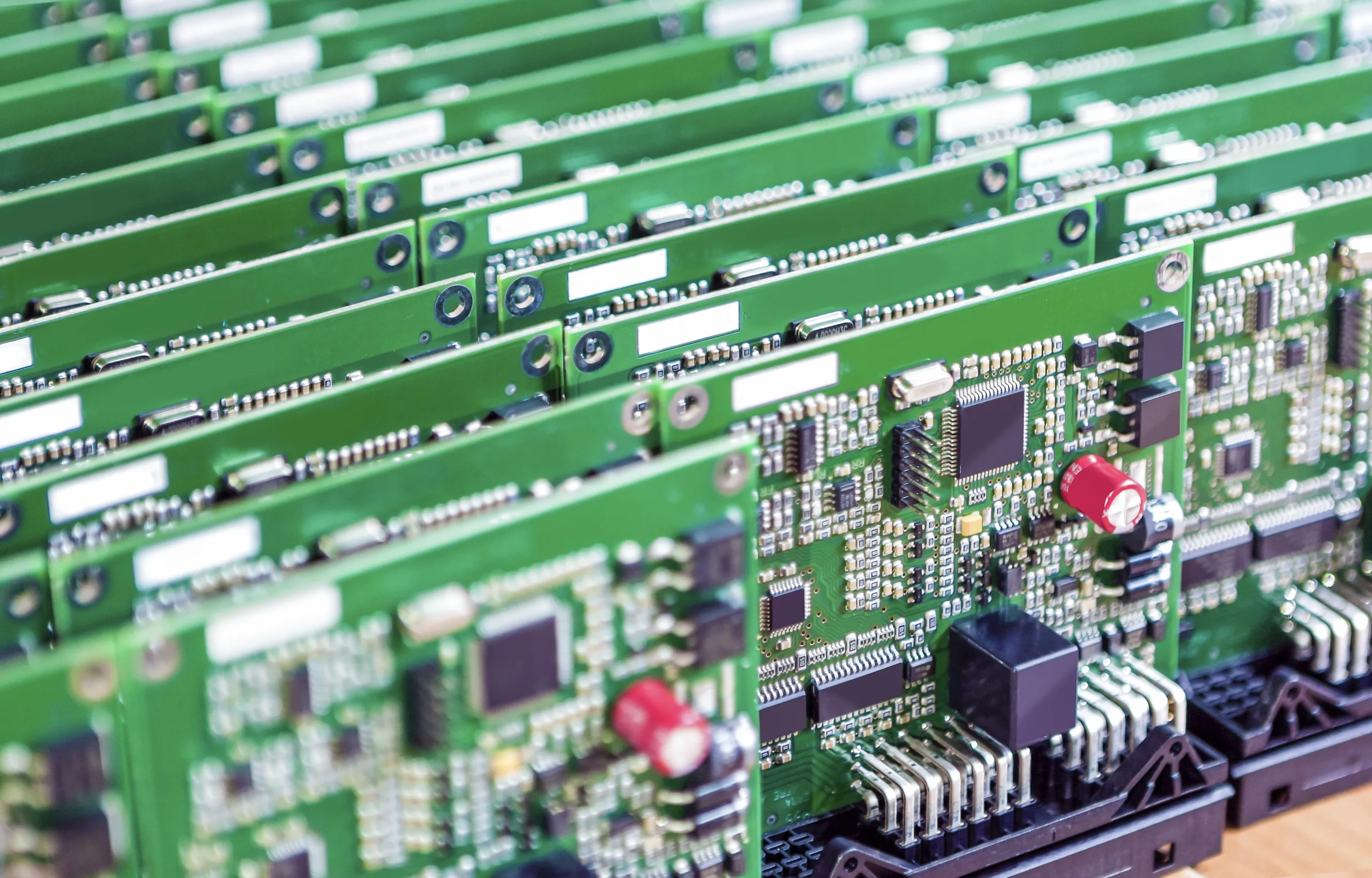
High Frequency Hybrid Product Classification:
- 레이어: 6
- 중고 보드: RO4350B + FR4
- 두께: 1.6mm
- 크기: 210mm x 280mm
- 표면 처리: 금도금
- 최소 조리개: 0.25mm
- 애플리케이션: 의사소통
- 특징: 고주파 혼합 압력
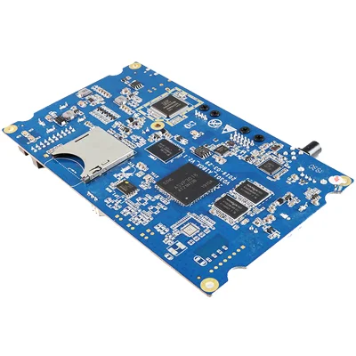
We provide Communication motherboard Turnkey PCB Assembly services. UGPCB is your one-stop Turnkey PCB Assembly company.


