
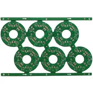
High-Density Double-Sided LED PCB: A Professional Lighting Solution with Enhanced Reliability
Modern compact consumer electronics and complex circuit designs demand higher PCB space efficiency, which traditional single-sided boards struggle to meet due to routing limitations. Double-sided PCB technology maximizes space utilization by providing conductive paths on both sides of the board, enabling tighter routing and component placement.
Cross-section diagram of a double-sided LED PCB showing top and bottom copper layers with plated through-holes.
01 핵심 정의 & 기술 사양
A double-sided LED PCB is a 인쇄 회로 기판 with conductive copper traces on both sides of the substrate. This design allows circuits and routing on each side, with electrical connections between layers established via plated through-holes (PTH). Unlike single-sided boards, double-sided PCBs resolve trace crossover challenges, offering greater design flexibility.
UGPCB’s double-sided LED PCBs use FR4 material—an epoxy-based substrate with excellent electrical insulation and mechanical strength. Standard specifications include a 1.0mm board thickness, 1온스 (대략. 35μm) 구리 두께, 그리고 OSP (유기 용해성 보존) 표면 마감. With a minimum trace width/spacing of 6mil (0.15mm), these PCBs support high-density routing within limited spaces, meeting complex LED layout requirements.
02 Core Structure & 작동 원리
The double-sided PCB structure consists of two conductive layers (top and bottom) and an inner insulation layer. Compared to single-sided boards, routing density can increase by approximately 60%–80%, effectively reducing product size.
UGPCB’s double-sided LED PCBs ensure interlayer conductivity via metallized through-holes. These holes, plated or filled with metal, act as “bridges” connecting traces on both sides. UGPCB employs advanced electroless copper deposition to form a reliable conductive layer on hole walls, ensuring robust double-sided conductivity.
Power and signal lines are carefully designed, allowing LED units to be mounted on both sides for dual-side display effects. Shield layers can also be added between adjacent boards to effectively filter out optical interference.
03 성능상의 이점 & 주요 특징
UGPCB’s double-sided LED PCBs offer several notable advantages over traditional single-sided boards.
-
Doubled Space Efficiency: 구성요소 can be placed on both top and bottom sides, doubling available area and enabling more complex circuits within the same footprint.
-
탁월한 신호 무결성 & 열 성능: Well-planned trace layouts across layers reduce signal interference and crosstalk. The dual-sided structure also provides more thermal management options—proper heat dissipation design and thermal vias help dissipate heat from sensitive components.
-
비용 효율성: Compared to single-sided boards, double-sided PCBs can save 30%–50% on material costs, making them especially suitable for small to medium batch production. Greater design freedom—such as cross routing and grid-based copper pours—offers engineers enhanced flexibility.
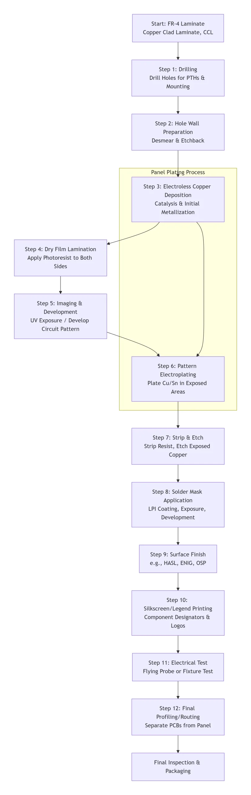
04 Professional Manufacturing Process
Double-sided LED PCB manufacturing is a multi-step precision process. It begins with an FR4 laminate—a dielectric substrate sandwiched between two thin copper layers to form conductive paths.
In the imaging stage, photoresist is applied to the copper layers. UV light transfers the circuit pattern onto the PCB, after which unexposed resist is washed away, exposing copper for etching.
During etching, a chemical etchant removes unwanted copper, leaving only the desired traces on each layer.
Drilling and plating are critical for interlayer connections. Holes are drilled for component mounting and layer interconnection, then plated with copper to ensure conductivity. A solder mask is applied across the entire PCB surface except exposed pads and traces to prevent solder bridging.
UGPCB utilizes advanced metallized hole technology, forming a reliable conductive layer on hole walls via electroless copper deposition. This includes both thin-copper thickening electroplating and thick-copper direct transfer methods.
05 응용 시나리오
This double-sided LED PCB is primarily used in the lighting industry, especially in LED applications requiring frequent switching. It effectively handles heat generated by high current and voltage cycles.
06 설계 지침 & Selection Tips
Designing a double-sided LED PCB requires attention to several key factors:
-
구성 요소 배치: Place related components on the same side where possible, while considering board thickness and thermal needs.
-
Routing Channel Planning: Carefully plan channels to isolate critical signals and avoid crosstalk. Use wider spacing between traces or ground planes as barriers.
-
레이어 스택업: Arrange similar signals together. 일반적으로, route critical traces on the top layer first, followed by a ground plane below.
-
Via Usage: Minimize via count to save costs while ensuring sufficient space for required connections.
-
Trace Length Matching: Essential for controlling skew and timing, especially for differential pairs and high-speed traces.
UGPCB offers professional PCB 설계 support to help optimize double-sided LED PCB 레이아웃. We recommend considering thermal management early in the design phase—ensuring proper heat dissipation and adequate spacing between heat-generating components.
07 Comparison with Special Substrate Materials
Although this LED PCB is fabricated on FR-4 substrate, we also provide services for special substrates like aluminum-based PCBs to meet diverse application needs. Aluminum substrates are metal-core clad laminates with excellent thermal conductivity, typically composed of three layers: 회로층 (구리박), 절연층, and metal base.
Compared to traditional FR4, aluminum substrates minimize thermal resistance and offer superior heat dissipation. For high-end applications, they can also be designed in a double-sided structure: circuit–insulation–aluminum base–insulation–circuit.
Aluminum substrates are ideal for high-power LED applications where significant heat is generated. Heat from surface-mounted power devices on the circuit layer transfers rapidly through the insulation to the metal base, enabling efficient thermal management—a key advantage over conventional FR4 PCBs.


