

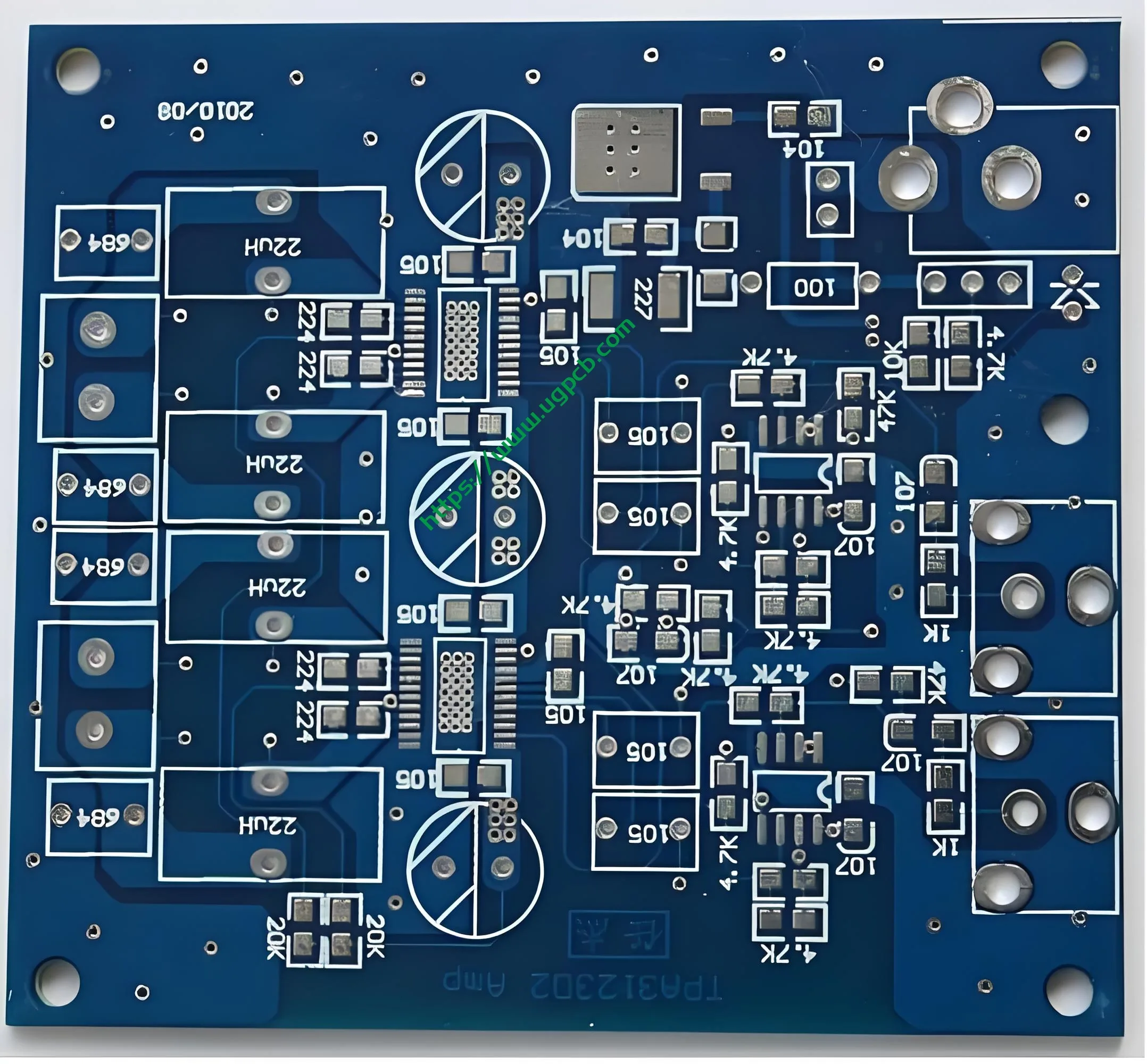
계전기 보호용 UGPCB 양면 PCB 소개
UGPCB는 고성능 제조 전문업체입니다. 양면 인쇄 회로 기판 (PCB) 계전기 보호 시스템에 맞게 맞춤화됨. 이 PCB는 다음과 같이 설계되었습니다. FR-4 에폭시 유리 천 으로 기본 자료, 우수한 전기 절연성 및 기계적 내구성 보장. 1.6mm의 마감 두께와 1oz의 구리 두께가 특징 (약 35μm), 이 보드는 강력한 전류 전달 용량을 지원합니다.. 그만큼 OSP (유기 용해성 보존) 표면 처리 구리 패드를 산화로부터 보호하면서 납땜성을 향상시킵니다.. 최소 트레이스와 8mil의 간격 (0.2mm), UGPCB의 설계는 정밀 구동 계전기 보호 애플리케이션을 위한 최적의 신호 무결성을 달성합니다.. 검정색과 흰색 솔더 마스크 색상 모두 사용 가능, 이 PCB는 다음을 준수합니다. CTI600 표준, 습한 조건에서 전기적 고장을 방지하기 위해 높은 비교 추적 지수 성능 제공.
양면 PCB 란 무엇입니까??
에이 양면 PCB 절연 기판의 양면에 전도성 구리 층을 통합합니다., ~와 같은 FR-4. 레이어는 다음을 사용하여 상호 연결됩니다. 도금된 관통 구멍 (PTHS) 또는 vias, 복잡한 회로를 컴팩트한 형태로 구현. 단면 PCB와 달리, 양면 변형은 더 높은 수준을 허용합니다. 구성 요소 밀도 및 레이아웃 유연성, 릴레이 보호 시스템과 같은 중간 수준의 복잡성 장치에 이상적입니다.. 이 보드는 지원합니다 양면 조립, 스루홀 및 표면 실장 기술 포함 (SMT), 산업 현장에서 널리 사용됩니다., 통신, 자동차 전자제품.
릴레이 보호 PCB 설계 지침
-
추적 너비와 간격: UGPCB 최소한의 권장 사항 8밀 (0.2mm) 트레이스 너비 및 간격 단락 위험을 완화하고 고전압 환경에서 신호 선명도를 보장합니다. .
-
열 완화 패드: 사용 십자형 열 패드 납땜 중 열을 발산하기 위한 넓은 구리 영역, 가상 관절의 위험 감소 .
-
사양을 통해: 안정적인 층간 연결을 위해, 최소 마감 구멍 직경이 0.3mm이고 환형 링이 0.7mm 이상인 PTH를 지정합니다. .
-
격자무늬 구리 비행기: 웨이브 솔더링 중 PCB 뒤틀림을 최소화하기 위해 간격이 ≥10mil인 그리드형 접지면을 구현합니다. .
-
솔더 마스크 세부사항: 브리징을 방지하고 열 패드를 노출시키기 위해 설계 파일의 솔더 마스크 레이어를 사용하여 솔더 마스크 개구부를 정확하게 정의합니다. .
릴레이 보호에서 양면 PCB가 작동하는 방식
릴레이 보호 시스템에서, 양면 PCB는 다음과 같은 기능을 합니다. 중추신경계, 전기 매개변수를 모니터링하고 오류 발생 시 연결 해제를 트리거합니다.. 듀얼 레이어 레이아웃은 통합을 용이하게 합니다. 전류 센서, 마이크로프로세서, 통신 모듈. 예를 들어, 최상층의 트레이스는 저전압 제어 신호를 전달할 수 있습니다., 하단 레이어는 고전류 경로를 처리하는 반면. 홀을 통해 도금 레이어 간 저임피던스 연결 생성, 신속한 결함 감지 및 대응 보장. 그만큼 CTI600 등급 기판 전도성 양극 필라멘트에 저항 (CAF) 형성, 이는 습도가 높은 환경에서 수명을 연장하는 데 매우 중요합니다..
UGPCB의 릴레이 보호 PCB 응용
UGPCB의 양면 PCB는 다음 위치에 배치됩니다.:
-
전력망 릴레이 시스템: 과전류 및 지락 보호용.
-
산업용 제어 패널: 제조 공장의 기계 모니터링.
-
재생에너지 인버터: 태양광/풍력 변환기 보호.
-
통신 인프라: 기지국 전원 공급 장치 보호.
-
철도 신호 시스템: 오류 없는 트랙 전환 보장.
양면 PCB의 분류
-
재료로: FR-4 (기준), CEM-3 (중간 범위), 및 폴리이미드 (고온).
-
표면 마감별: OSP (UGPCB의 기본값), HASL, 동의하다, 그리고 침수 주석.
-
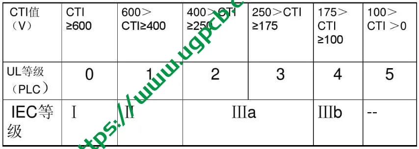
CTI 등급별: CTI600 (UGPCB의 보드처럼), CTI400, 열악한 환경을 위한 CTI600+.
재료 및 건설
-
기본 재료: FR-4 유리 에폭시 그것의 위해 사용됩니다 난연성 (UL94V-0) 절연 내력 .
-
구리 포일: 전해 구리 1온스 두께 (35μm) 면당 .
-
솔더 마스크: 사용 가능 검정색 또는 흰색, Taiyo PSR-4000 시리즈 기반, ≥10μm 절연 두께 제공 .
-
표면 마감: OSP는 구리 패드에 보호 유기층을 형성합니다., 무연 납땜성 보장 .
핵심 성과 지표
-
유전 강도: 전도성 층 사이의 고전압을 견딥니다..
-
열 내구성: 유리전이온도 (Tg) 130~145°C 하중에 따른 변형을 방지합니다. .
-
CTI 등급: CTI600 최대 600V까지 추적에 대한 저항 보장.
-
변형 공차: 최대 변형 또는 0.7% SMT 조립 보드용 .
-
도금된 스루홀 신뢰성: 홀 내 구리 도금 ≥20μm로 중단 없는 층간 연결 보장 .
Structure of a Double-Sided PCB
UGPCB’s PCBs feature:
-
Top and Bottom Copper Layers: 35μm thick, etched into circuit patterns.
-
FR-4 Core: A 1.6mm thick insulating substrate.
-
도금된 관통 구멍: Metallized with copper for layer interconnection.
-
솔더 마스크 층: Applied over copper, excluding solderable pads.
-
실크스크린 전설: White or black markings for component placement.
Advantages of UGPCB’s Design
-
비용 효율성: Reduces material expenses by 30–50% compared to multilayer alternatives.
-
Enhanced Design Flexibility: Supports cross-routing and optimized grounding schemes.
-
향상된 열 관리: Gridded copper planes and thermal vias dissipate heat efficiently.
-
높은 신뢰성: CTI600 and OSP finish extend service life in demanding conditions.
Manufacturing Process Overview
-
재료 준비: Cut FR-4 substrate to 510x610mm panels.
-
교련: CNC drills create holes as small as 0.2mm for PTHs .
-
Electroless Copper Deposition: Catalytic oxidation builds a conductive layer in holes .
-
패턴 이미징: 포토리소그래피는 UV 노출을 사용하여 회로 레이아웃을 전송합니다..
-
전기도금: 구리 증착으로 트레이스와 홀 벽이 20μm 이상으로 두꺼워집니다. .
-
에칭: 불필요한 구리 제거, 추적 정의.
-
솔더 마스크 적용: UV 경화형 잉크 인쇄 및 개발.
-
OSP 코팅: 노출된 구리에 유기 방부제 도포.
-
실크스크린 인쇄: 구성 요소 표시가 추가되었습니다..
-
라우팅 및 V-스코어링: 개별 보드로 분리된 패널.

일반적인 사용 시나리오
-
유틸리티 변전소: 변압기 및 피더용 하우징 보호 계전기.
-
산업용 모터 드라이브: 과부하 방지를 위한 제어 로직 내장.
-
무정전 전원 공급 장치 (UPS): 배터리 충전/방전 주기 관리.
-
스마트 미터: 실시간 에너지 모니터링 활성화.

결론
UGPCB의 계전기 보호용 양면 PCB 기판 결합 고급 재료, 정밀공학, 그리고 엄격한 테스트 비교할 수 없는 신뢰성을 제공하기 위해. 다음과 같은 기능을 갖춘 FR-4 단열재, OSP 코팅, 및 CTI600 준수, 중요한 전력 시스템을 위한 최적의 선택입니다.. 장비 안전성과 수명을 향상시키려는 엔지니어는 다음 프로젝트에 UGPCB의 전문 지식을 활용할 수 있습니다..


