
Overview of 6 Layer Golden Finger PCB
그만큼 6 Layer Golden Finger PCB is a high-precision, multi-layered printed circuit board designed for advanced electronic applications. This product combines multiple layers of conductive traces and insulating materials to provide exceptional performance and reliability in various electronic devices.
정의
에이 6 Layer Golden Finger PCB is a type of multi-layer printed circuit board (PCB) that features six individual layers of conductive material, 절연 층으로 분리됩니다. 용어 “황금 손가락” refers to the specific surface treatment applied to the edges of the board, which involves immersion gold and additional gold plating on the contact fingers.
설계 요구 사항
When designing a 6 Layer Golden Finger PCB, several key requirements must be considered:
- 재료 품질: High-quality FR4 material is essential for durability and performance.
- 레이어 구성: Six layers are needed to accommodate complex circuitry and signal routing.
- 구리 두께: A standard copper thickness of 1OZ ensures adequate conductivity.
- 표면 처리: Immersion gold with additional gold finger plating enhances connectivity and corrosion resistance.
- 추적/공간 차원: A minimum trace/space of 4mil/4mil is required for precise circuit patterns.
- 특수 공정: The gold finger process with a thickness of 0.1um is critical for reliable edge connections.
작동 원리
그만큼 6 Layer Golden Finger PCB operates based on the principles of electrical conductivity and insulation. Conductive traces on different layers create pathways for electrical signals, 절연층은 이러한 신호 간의 원치 않는 상호 작용을 방지합니다.. The gold finger edges facilitate easy insertion into connectors, ensuring stable and reliable connections.
응용
This type of PCB is widely used in applications that require high precision and reliability, ~와 같은:
- High-speed digital circuits
- 통신 장비
- Advanced computing systems
- 자동차 전자 제품
- 의료기기
분류
6 Layer Golden Finger PCBs can be classified based on their intended use, ~와 같은:
- 신호 처리 보드: 통신 장치에서 고주파 신호를 처리합니다.
- 발전 보드: 복잡한 전자 시스템에서 전원 공급 장치를 관리합니다.
- 제어 보드: For controlling and managing various functions in electronic devices.
재료
a 6 Layer Golden Finger PCB include:
- 기본 재료: FR4, 우수한 유전 특성과 기계적 강도로 유명한 난연성 유리 섬유 소재.
- 전도성 재료: 구리, 전도성 트레이스에 사용됨.
- 표면 처리: Immersion gold and additional gold plating for the gold fingers.
성능
a의 성능 6 Layer Golden Finger PCB is characterized by:
- 높은 신호 무결성: 정확한 추적/공간 치수 및 고품질 재료로 인해.
- 안정적인 연결: Ensured by the gold finger surface treatment.
- 내구성: Enhanced by the robust FR4 base material and immersion gold finish.
- 전기 효율성: 최적화된 레이어 구성으로 신호 손실 및 간섭 최소화.
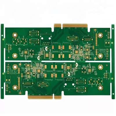
구조
a의 구조 6 Layer Golden Finger PCB consists of:
- 6개 층의 전도성 재료: 절연층과 교대로 사용.
- Gold Finger Edges: Plated with a thin layer of gold for enhanced connectivity.
- Protective Layers: Including solder mask and silkscreen for protection and identification.
특징
Key features of the 6 Layer Golden Finger PCB include:
- 고급 표면 처리: Immersion gold plus gold finger for superior connection quality.
- 높은 정밀도: With a minimum trace/space of 4mil/4mil.
- 사용자 정의 가능한 색상 옵션: 녹색 또는 흰색으로 제공됩니다..
- 표준두께: 1.6mm의 마감두께로.
생산 과정
The production process for a 6 Layer Golden Finger PCB involves several steps:
- 재료 준비: FR4 시트 및 동박 선택 및 준비.
- 레이어 스태킹: 구리와 절연 재료의 교대 층.
- 에칭: 원하는 회로 패턴을 형성하기 위해 여분의 구리를 제거합니다..
- 도금: Applying immersion gold and additional gold finger plating.
- 라미네이션: 열과 압력 하에서 층 결합.
- 교련: 관통 구멍 구성요소 및 비아용 구멍 생성.
- 솔더 마스크 적용: 솔더 브리지 및 환경 요인으로부터 회로 보호.
- 실크스크린 인쇄: 구성 요소 배치 및 식별을 위한 텍스트 및 기호 추가.
- 품질 관리: PCB가 모든 설계 사양 및 표준을 충족하는지 확인.
시나리오 사용
그만큼 6 Layer Golden Finger PCB is ideal for scenarios where:
- 높은 신호 무결성이 중요합니다.
- 안정적이고 내구성 있는 연결이 필요합니다..
- 공간 제약으로 인해 컴팩트하고 효율적인 디자인이 필요합니다..
- 성능 향상을 위해서는 고급 표면 처리가 필요합니다..


