
1. 제품개요: Where High-Frequency Performance Meets Cost-Effectiveness
In today’s rapidly evolving landscape of 5G communication, 마이크로파 레이더, and aerospace electronics, the material selection for PCB (인쇄 회로 기판) directly determines the performance ceiling of end-user equipment. To meet the stringent signal integrity requirements of RF (무선 주파수) and high-speed digital circuits while controlling manufacturing costs, hybrid laminate PCB technology has emerged as a vital solution.
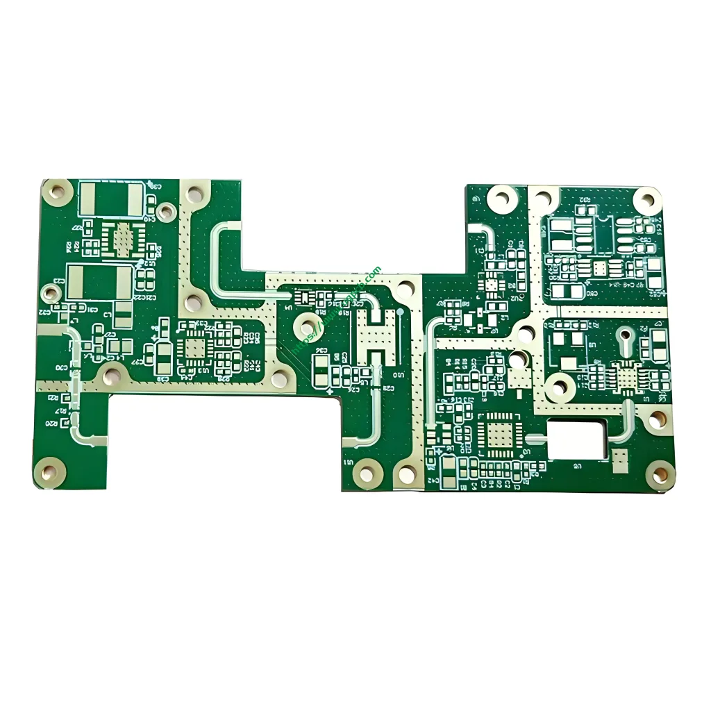
UGPCB Rogers RO4350B 하이브리드 PCB represents the pinnacle of this technological approach. This product ingeniously combines Rogers RO4350B high-frequency laminates with conventional FR-4 materials through precise construction design, creating a 4-layer board that delivers both exceptional high-frequency characteristics and mechanical stability. With a stable 유전 상수 (DK) ~의 3.48 and a precisely controlled finished board thickness of 1.0mm, complemented by 이머젼 골드 (동의하다) 표면 마감, this PCB is engineered specifically for communication equipment demanding ultimate signal transmission quality.
2. Product Definition and Scientific Classification
정의: UGPCB’s Rogers RO4350B Hybrid PCB is a mixed dielectric laminate printed circuit board. It features an asymmetric “2-layer Rogers RO4350B + 2-layer FR4” 건설, integrating high-frequency materials with standard materials within a single board.
과학적 분류:
-
재료로: Rigid Board, Mixed Dielectric Laminate
-
By Operating Frequency: High-Frequency Microwave Board
-
By Process Structure: 다층 PCB, specifically 4-layer configuration
3. Core Technical Parameters and Design Considerations
UGPCB strictly adheres to material specifications in the design of this product, ensuring every board precisely matches the requirements of RF front-end module designs:
-
Core Construction (구조): 2 Layers Rogers RO4350B + 2 Layers FR4. This configuration places RO4350B on the outer layers for high-frequency signal transmission, while FR4 serves as inner or bottom layers providing mechanical support and power distribution, 성능과 비용 간의 최적의 균형 달성.
-
유전 상수 (DK): 3.48 (typically tested at 10GHz). RO4350B’s Dk exhibits minimal variation with frequency and temperature changes, ensuring phase stability of high-frequency signals.
-
Physical Dimensions:
-
레이어 수: 4 레이어
-
완성된 두께: 1.0mm
-
유전체 두께: 0.508mm (typically referring to the RO4350B core layer thickness, critical for impedance control)
-
-
Copper Thickness Configuration:
-
재료 구리 두께: ½ oz (18μm) HH/HH, meaning all layers start with 0.5 oz copper foil.
-
완성된 구리 두께: 1/0.5/0.5/1 (온스). This precise layer-specific copper thickness design delivers:
-
L1 & L4 (외부 층): 1 온스 (35μm), enhancing current-carrying capacity and outer layer soldering reliability.
-
L2 & L3 (내부 레이어): 0.5 온스 (18μm), facilitating fine-line etching and ensuring signal layer precision.
-
-
-
표면 처리: 이머젼 골드 (동의하다). ENIG provides excellent surface planarity—critical for high-frequency signal transmission where skin effect dominates—while offering superior oxidation resistance and solderability.
-
가연성 등급: UL 94 다섯-0 준수, ensuring product safety.
4. 작동 원리 및 성능 이점
작동 원리
As a carrier and electrical interconnection platform for electronic components, this PCB operates on a fundamental principle: high-frequency signals travel through microstrip or stripline structures within the Rogers RO4350B material layers (L1, L2). Thanks to RO4350B’s exceptionally low 소산 인자 (Df) and stable dielectric constant, signal energy loss during transmission is minimized, with reflections and scattering effectively suppressed. The underlying FR4 layers primarily handle power distribution and digital control signal transmission, interconnected through precisely designed vias without mutual interference.
Core Performance Advantages
-
탁월한 신호 무결성: Rogers RO4350B material ensures low insertion loss and high signal transmission speed, perfectly meeting 5G communication requirements for high data rates.
-
Excellent Temperature Stability: RO4350B features a high glass transition temperature (Tg) and an exceptionally low Z-axis coefficient of thermal expansion (CTE), ensuring plated through-hole (PTH) reliability under extreme temperature variations and preventing barrel cracking.
-
Optimized Power and Thermal Management: The asymmetric copper thickness design (1oz outer layers) facilitates heat dissipation from high-power components. RO4350B’s thermal conductivity, 약 0.69 W/m·k, exceeds that of standard FR4, effectively drawing heat away from hotspots.
-
Mechanical and Process Compatibility: Unlike pure ceramic or PTFE materials, RO4350B is rigid and highly compatible with FR4 processing workflows, supporting conventional CNC drilling and copper deposition processes for volume production.
5. 제조 공정 흐름
UGPCB employs a rigorously controlled process flow to ensure the quality of this mixed dielectric PCB:
-
Incoming Material Inspection: Strictly source original Rogers RO4350B laminates and grade A FR4 materials (such as SYTECH or equivalent), verifying Dk values and resin flow characteristics.
-
Inner Layer Circuitry (L2/L3): Apply dry film to 0.5oz inner layer copper, followed by exposure, 개발, and acid etching to form precision circuits.
-
Brown Oxide and Lamination: Critical process! Stack inner layer cores, 준비, and outer layer RO4350B/copper foil according to construction specifications. Due to differing resin flow characteristics of RO4350B and FR4, stepped temperature profiles during lamination are essential to prevent delamination and voids.
-
교련: Utilize ultra-hard coated drill bits with optimized speed and feed rates to minimize wear from glass fiber and ceramic fillers in RO4350B material, ensuring smooth hole walls.
-
Electroless Copper and Panel Plating: Achieve interlayer interconnection and increase outer layer copper thickness to 1oz through pattern plating, with hole copper thickness meeting IPC Class 2/3 표준.
-
Outer Layer Circuitry: Fabricate precision RF microstrip or antenna traces on L1 and L4.
-
Solder Mask and Legend: Apply high-quality photosensitive solder mask ink to protect circuits and prevent signal leakage.
-
표면 마무리: 이머젼 골드 (동의하다) 프로세스. Apply a uniform chemical nickel-gold layer on pads for excellent solderability.
-
Profiling and Electrical Testing: CNC routing for final shape, 이어서 100% flying probe testing or dedicated fixture testing, with special focus on 임피던스 제어 verification within specified tolerances.
6. 일반적인 응용 프로그램 시나리오
With its stable Dk value of 3.48 그리고 mixed dielectric construction, UGPCB’s product is primarily applied in the following high-frequency communication fields:
-
기지국 안테나: 5G Massive MIMO antenna arrays, 전력 증폭기
-
위성 통신: LNB (Low-Noise Block downconverters), GPS active antennas
-
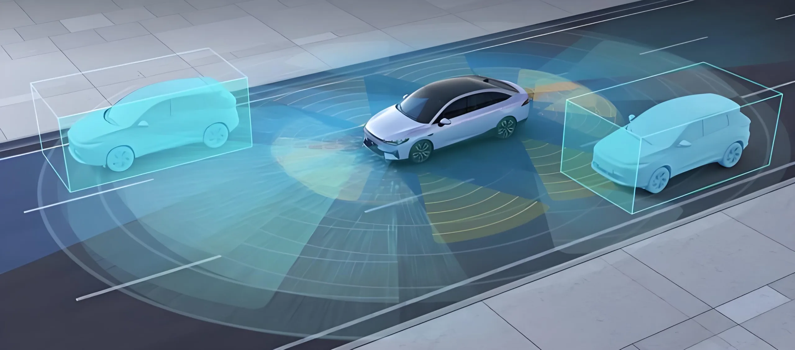
자동차 전자: 77GHz 밀리미터파 레이더, in-vehicle infotainment high-frequency modules
-
산업 제어: High-frequency data acquisition equipment, wireless bridge devices
-
Test and Measurement: Internal high-frequency boards for network analyzers, RF probe cards
7. UGPCB를 선택하는 이유는 무엇입니까??
-
Precise Parameter Replication: We understand that data is critical. We commit to strict adherence to your PCB 설계 documentation, ensuring RF performance aligns with simulation designs.
-
Expert Hybrid Lamination Technology: With over a decade of experience in mixed dielectric board processing, we have mastered RO4350B and FR4 matching flow control techniques, eliminating process challenges such as delamination and warpage.
-
Rapid Response and Service: Comprehensive support from PCB 레이아웃 review and impedance calculation to prototyping and small-batch production.
Ready to Elevate Your RF Design?
Partner with UGPCB as your most reliable 고주파 PCB manufacturing ally. Whether for 5G communications, 레이더 시스템, or precision instrumentation, 우리의 Rogers RO4350B 하이브리드 PCB delivers stable, 효율적인, and cost-effective hardware support.
Please send the following specifications to our sales team:
-
모델: Rogers RO4350B 하이브리드 PCB
-
Quantity: [Your required quantity]
-
특별 요구 사항: [예를 들어, impedance trace tolerances, packaging preferences]
| Key Parameter | 사양 | 용인 |
|---|---|---|
| 레이어 수 | 4 레이어 | – |
| 구조 | 2 Layers RO4350B + 2 Layers FR4 | – |
| 유전 상수 (DK) | 3.48 | ± 0.05 |
| 완성된 두께 | 1.0 mm | ± 10% |
| Outer Layer Finished Copper | 1 온스 (35μm) | – |
| Inner Layer Finished Copper | 0.5 온스 (18μm) | – |
| 표면 마감 | 이머젼 골드 (동의하다) | – |
Contact UGPCB Experts: Request Quote | [이메일: sales@ugpcb.com]


