UGPCB 화학 연구실: PCB 제조의 핵심 기술 엔진
소개
전자 제조 산업에서, 인쇄 회로 기판 (PCB) 전자 제품의 기본 캐리어 역할, 품질이 최종 제품의 성능과 신뢰성에 직접적인 영향을 미칩니다.. PCB 분야의 선두주자로서, PCB, 그리고 PECVD 서비스, UGPCB는 재료 분석 등 핵심 기능을 수행하는 화학 실험실을 운영합니다., 프로세스 최적화, 품질 관리. 이 기사에서는 연구소 운영 시스템에 대한 심층 분석을 제공하고 PCB 제조에서 중요한 역할을 강조합니다..
연구실 레이아웃 및 장비 시스템
중앙실험구역
그만큼 UGPCB 연구소는 다음과 같은 핵심 영역을 갖춘 모듈식 설계를 채택합니다.:
중앙실험구역
-
강산과 알칼리에도 견딜 수 있도록 EPOXY 수지로 표면 처리된 부식 방지 작업대 장착. 비커, 메스실린더 등 유리기구가 가지런히 배열되어 있습니다., 시약병은 카테고리별로 파란색 트레이에 보관되어 있습니다., 5S 경영 구현.
환기 시스템
-
여러 개의 흄후드에 연결된 빨간색 배기 덕트는 다음과 같은 공기 흐름 속도를 보장합니다. 0.5 밀리미터/초, 유기용제 증기 유지 (예를 들어, 아세톤, 이소프로필 알코올) 직업적 노출 한계 미만의 농도.
정밀검사구역
-
분광 광도계로 구성 (구리 이온 농도 검출용), 원자흡광분광계 (중금속 잔류물 분석용), 및 XRF 코팅 두께 측정기 (정확도 ±0.1μm). 장비 간격은 ISO를 준수합니다. 14644-1 클린룸 표준.
핵심 PCB 공정 분석
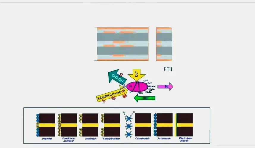
PCB 무전해 동도금 공정
이 과정은 3단계 반응 메커니즘을 따릅니다.:
전처리 (알칼리성 과망간산 칼륨 시스템)
MnO₄⁻ + H2O → MnO2 + 2오⁻ + O²↑
초음파 세척으로 수지 잔여물을 제거합니다. PCB 구멍 벽, 거칠기는 Ra 0.15–0.3 μm로 제어됩니다..
활성화 (콜로이드 팔라듐 시스템)
Pd²⁺ + Sn²⁺ → Pd-Sn 콜로이드 입자
초음파 보조로 마이크로비아에서 균일한 촉매 흡착 보장 (≥0.15mm) 내벽.
구리 증착 (포름알데히드 감소 시스템)
cu²⁺ + HCHO + OH⁻ → Cu↓ + HCO⁻ + H2O
주요 매개 변수: pH 9.0~9.5, 온도 30±0.5°C, 증착률 2 μm/15분, 구리 두께 ≥1.5μm (IPC-6012 표준에 따라).
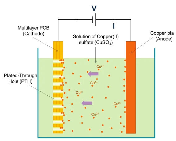
PCB 전기도금 공정 최적화
Hull Cell을 사용하여 생산 조건 시뮬레이션, 다음 반응은 도금 균일성을 보장합니다.:
양극: Cu → Cu²⁺ + 2이자⁻
음극: cu²⁺ + 2e⁻ → Cu↓
주요 매개 변수: 전류 밀도 1.5 A/dm², 목욕 온도 25±1°C, PCA 5~8ml/L로 유지되는 첨가제 농도, 구멍 벽의 구리 두께 편차 ≤5% 보장.
안전 및 품질 관리 시스템
실험실 안전 프로토콜
-
보호 조치: 작업자는 니트릴 장갑을 착용합니다., 고글, 그리고 정전기 방지 앞치마; 강산 취급 시 안면 보호대 추가.
-
폐액 처리: 구리 함유 폐기물은 이온 교환 수지를 통해 재활용됩니다. >60% 회복율; 유기 폐기물은 공장에 들어가기 전에 활성탄 흡착으로 처리됩니다. RTO 소각 시스템.
-
비상관리: 비상 세안 스테이션과 샤워 시설을 갖추고 있습니다.; 가장 가까운 소방서의 대응 시간은 3분 이내입니다..
실시간 모니터링 시스템
-
온라인 분석: 전도도 측정기는 도금조의 불순물을 모니터링합니다.; Cl⁻ 농도가 초과되면 자동 순수 보충이 시작됩니다. 50 ppm.
-
추적성 관리: 각 배치 기록에는 시약 로트 번호가 포함됩니다., 장비 교정 날짜, 및 운영자 서명, ISO 준수 17025 실험실 인증 요구 사항.
산업 응용 및 기술 혁신
PCB 표면처리 공정 비교
| 프로세스 유형 | 응용 시나리오 | 주요 매개변수 |
|---|---|---|
| 동의하다 | 고밀도 상호 연결 (BGA/CSP) | 니켈 두께 3~5μm, 금 두께 0.05–0.1 μm |
| OSP | 가전제품 (모바일/태블릿) | 필름 두께 0.2~0.5μm, 유통기한 6개월 이하 |
| 침수 주석 | 자동차 전자 (고온 저항) | 주석 두께 1.0±0.2μm, 수염 비율 <2% |
획기적인 사례 연구
5G 통신보드 프로젝트의 경우, UGPCB는 동적 매개변수 보상 시스템을 구현했습니다., 달성:
-
30% 마이크로비아 구리 두께 균일성 향상 (CPK >1.33)
-
무전해 구리 용액 수명 연장: 120 m²/L (업계 평균: 80 m²/L)
-
100% 열충격 테스트 합격률 (288°C × 10초 × 3 사이클)
결론
UGPCB 화학 연구소는 정밀한 공정 제어를 통해 재료 분석부터 최종 제품 검증까지 엔드투엔드 품질 보증을 보장합니다., 철저한 안전관리, 그리고 지속적인 기술 혁신. 핵심 기술 매개변수는 IPC-4552A 및 JPCA-ET01과 같은 국제 표준을 충족합니다., 5G 기지국을 포함한 고급 애플리케이션에 대한 안정적인 지원 제공, 자동차 전자, 의료기기, 중국 PCB 제조의 앞선 역량 입증.


