
“Por que os chips ficam danificados quando eu apenas manuseio o placa de circuito normalmente?”Muitos engenheiros ficam confusos ao enfrentar danos no circuito causados por descarga eletrostática (ESD). Na verdade, o corpo humano pode gerar tensões eletrostáticas de até dezenas de milhares de volts – excedendo em muito o limite de tolerância da maioria dos componentes eletrônicos.
Mesmo a maior precisão PCB (Placas de circuito impresso) pode ser vulnerável a ESD. Um toque acidental pode fazer com que chips no valor de milhares de dólares falhem instantaneamente.
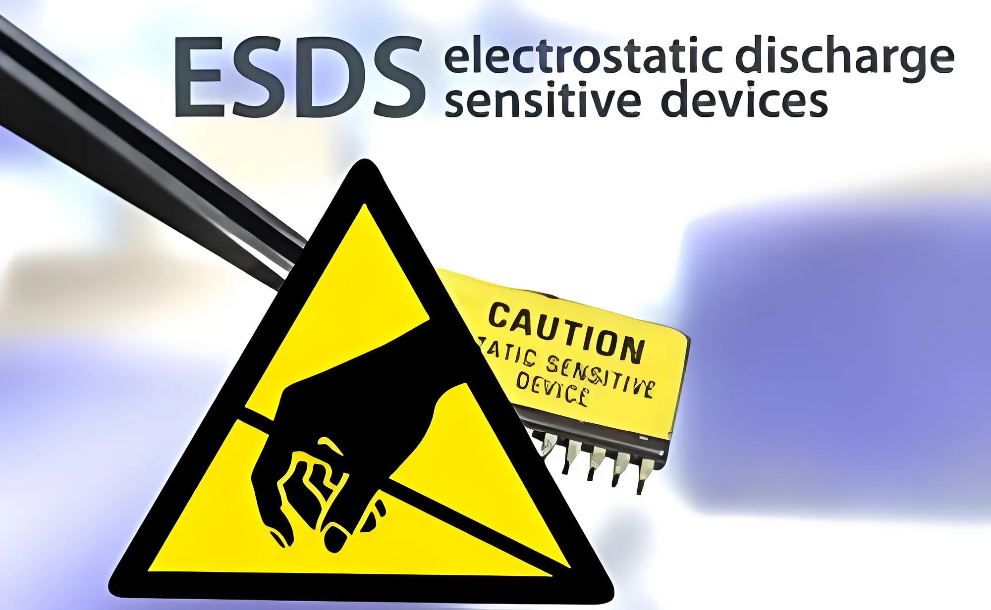
Contra o pano de fundo dos dispositivos eletrônicos cada vez mais sofisticados de hoje, A proteção ESD não é mais uma escolha opcional, mas uma medida necessária para garantir a confiabilidade do produto. Este artigo analisará profundamente os principais pontos de projeto e os críticos de fabricação da proteção ESD de PCB., ajudando seus produtos a resistir a esse “relâmpago invisível”.
1. Ameaças ESD: O impacto letal do relâmpago invisível em miniatura
ESD pode ser imaginado como um relâmpago em miniatura invisível. Atividades diárias, como caminhar, tirando suéteres, ou mesmo pegar uma caixa plástica pode gerar eletricidade estática. A voltagem desta eletricidade estática muitas vezes atinge vários milhares de volts, ou mesmo dezenas de milhares de volts.
O próprio corpo humano é na verdade o maior gerador de eletricidade estática. Especialmente nas estações secas, ESD pode ocorrer no momento em que você pega uma PCB. Itens aparentemente insignificantes, como mesas de plástico, tapetes de fibra química, e caixas de embalagem de espuma podem se tornar “cúmplices” da eletricidade estática.
ESD prejudica PCBs de duas formas principais:
- Danos graves: Este é o dano mais direto e óbvio. O ESD irá quebrar instantaneamente os minúsculos circuitos dentro do chip, causando danos permanentes ao chip. Como resultado, o PCB irá parar de funcionar completamente, ou funções específicas (como portas seriais ou ADCs) irá falhar diretamente.
- Danos crônicos: Isso é mais oculto e problemático. ESD pode não destruir completamente o chip, mas pode causar microdanos às camadas internas de óxido e outras estruturas. O PCB ainda pode funcionar normalmente agora, mas ficará instável e terá uma vida útil reduzida. Pode funcionar repentinamente após alguns dias ou sob temperaturas específicas. Essa falha intermitente é a mais difícil de solucionar durante a depuração e consome muito tempo e esforço.
2. Diodos TVS: O sistema de proteção contra raios de precisão para circuitos
TVS (Supressor de tensão transitória) os diodos são a primeira linha de defesa contra ameaças de ESD e os componentes de proteção mais eficazes. Eles agem como “guardas de segurança para sinais de circuito” – mantendo um estado de alta impedância em condições normais. Assim que um pulso ESD for detectado, eles mudam instantaneamente para um estado de baixa impedância, desviando o pulso de alta tensão para o solo e protegendo os chips backend.
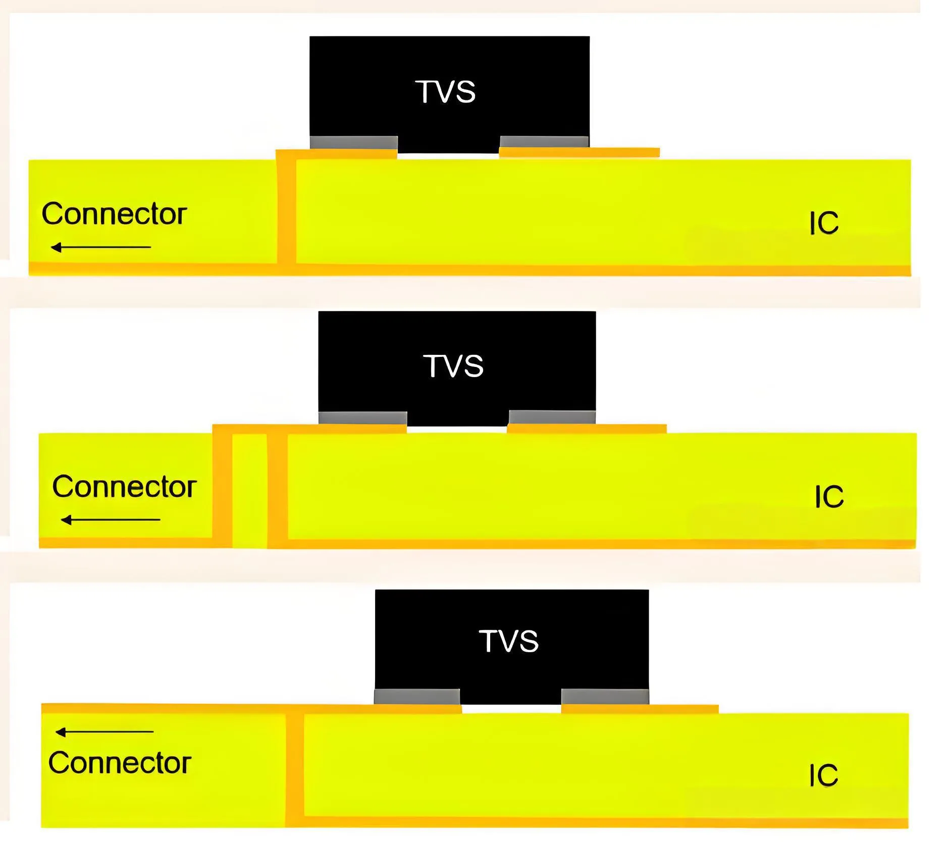
2.1 Regras de ouro para layout de TVS
A indutância parasita é o maior inimigo do desempenho do TVS. A indutância parasita no circuito – incluindo a indutância parasita dos próprios pinos TVS – afeta a tensão de fixação (Você) no back-end IC quando ocorrem ESD ou surtos.
O efeito protetor do TVS segue a fórmula: VCL = VBR + RD × IPP. Entre eles:
- RD é a capacitância parasita do próprio TVS; produtos com valores RD menores têm melhor tensão de fixação e podem proteger os CIs de forma mais eficaz.
- IPP é a corrente que passa pelo TVS durante o instante de teste.
Para maximizar o efeito de proteção do TVS, você deve garantir que a conexão de aterramento seja a mais curta possível e colocar o TVS o mais próximo possível da fonte ESD.. Isso não apenas minimiza a EMI (Interferência Eletromagnética) no PCB, mas também reduz o acoplamento com outros caminhos. A escolha de um dispositivo TVS com tempo de resposta inferior a 1ns fornece proteção ideal para interfaces de alta velocidade – fundamental para PCBA (Conjunto da placa de circuito impresso) confiabilidade.
3. Layout e aterramento da PCB: A Fundação da Proteção ESD
Razoável Layout da placa de circuito impresso e o projeto de aterramento são os pilares da proteção ESD. Mesmo sem componentes de proteção adicionais, eles podem melhorar significativamente a imunidade ESD do produto.
3.1 Pontos-chave para layout de PCB
- As linhas de sinal de alta velocidade devem estar ≥3 mm de distância da borda da placa, enquanto os sinais sensíveis de baixa frequência devem estar ≥2 mm de distância.
- Sinais críticos, como linhas de relógio e linhas de reinicialização, devem ser cercados por terra (blindagem de solo). Organize linhas de aterramento em ambos os lados e adicione vias de aterramento a cada 50 mm.
- Todos os invólucros metálicos expostos devem ser aterrados em ponto único através de um resistor de 1MΩ para evitar a formação de um circuito de baixa impedância através do aterramento direto.
- Uma distância de fuga de ≥5 mm deve ser mantida entre os componentes de contato do usuário (como botões e botões) e a placa principal. Use espuma condutora ou molas metálicas para obter conexão equipotencial.
- Definir centelhadores (com um espaçamento de 0,2 mm–0,5 mm) na posição Pin1 do conector e no ponto de aterramento do invólucro metálico. Estas medidas podem orientar eficazmente a corrente ESD para descarregar com segurança e evitar danos a circuitos sensíveis.
3.2 Princípios para projeto de aterramento de PCB
Ao projetar camada dupla ou PCB multicamadas, tente garantir um plano terrestre completo e de grande área. Um plano terrestre completo é como uma planície extensa – pode absorver e dispersar rapidamente a energia ESD, evitando que a energia se acumule em um único ponto. Ao mesmo tempo, fornece um caminho de descarga eficiente para diodos TVS.
Durante o layout do PCB, preencha a rede de aterramento com cobre e certifique-se de que o cobre de aterramento cubra o máximo da área vazia na placa (sem vestígios) possível. Para todas as interfaces externas (como portas USB e tomadas de energia DC), conecte o invólucro metálico ao terra da placa através de um capacitor de alta tensão ou diretamente. Por aqui, A ESD será desviada primeiro através do gabinete antes de entrar no circuito - melhorando a proteção ESD da PCB no nível da interface.
4. Processo de Laminação: A barreira de proteção interna para PCBs multicamadas
Em PCBs multicamadas, a qualidade do processo de laminação está diretamente relacionada à capacidade interna de proteção ESD da placa. Se o dielétrico entre duas camadas condutoras for muito fino, ESD de alta tensão pode facilmente quebrá-lo, causando danos permanentes.
4.1 Papel central do pré-impregnado
Predeg (material compósito pré-impregnado) atua como dielétrico isolante intercamada em PCBs multicamadas. É um “material compósito funcional” controlado por processos de fabricação de precisão, com sua principal característica sendo que a resina está em um “estado de semicura de estágio B” - uma característica que é fundamental para realizar a laminação de placas multicamadas.
Prepreg não apenas fornece ligação física, mas também atinge três efeitos: isolamento elétrico + suporte estrutural. Seu desempenho de isolamento e propriedades dielétricas determinam diretamente a confiabilidade elétrica do PCB: depois de curar, a resistividade do volume é ≥10¹⁴Ω·cm, e a resistência à tensão de ruptura é ≥20kV/mm, que pode bloquear o vazamento entre camadas – fundamental para evitar danos entre camadas induzidos por ESD.
Os parâmetros principais do Prepreg incluem:
- Conteúdo de resina (RC%): Normalmente 50%~70%, que determina a resistência de ligação entre camadas e a espessura da camada dielétrica.
- Fluidez: 15~30mm.
- Temperatura de transição vítrea (Tg): Normalmente 150~200℃.
- Constante dielétrica (Dk): 4.2±0,2 para pré-impregnado FR-4 comum.
4.2 Controle de Qualidade do Processo de Laminação
Para garantir a qualidade da laminação, o coeficiente de expansão térmica (CTE) do Prepreg deve corresponder ao das placas principais FR-4 e folhas de cobre. Se o desvio CTE do eixo Z exceder 5ppm/℃, é provável que ocorram fissuras entre camadas durante o ciclo de temperatura.
Durante a laminação:
- Quando a temperatura da camada intermediária é de 80 ~ 130 ℃, a diferença de temperatura entre a camada superior da placa transportadora e a camada intermediária não deve exceder 25 ℃, e a taxa de aquecimento não deve exceder 1,3~5℃/min.
- Quando a temperatura atinge 85±5℃, determinar o tempo para mudar de baixa pressão para média pressão.
- Quando a temperatura atinge 110±5℃, determinar o tempo para mudar de pressão média para alta pressão.
Na fabricação moderna de PCBs, a tecnologia de prensa a vácuo melhorou significativamente a qualidade da laminação. O ambiente de vácuo evita a formação de bolhas e vazios, garantindo fluxo e enchimento uniformes de resina pré-impregnada - fortalecendo a resistência do PCB multicamadas à quebra de ESD.
5. Processos Avançados e Verificação de Qualidade
À medida que os dispositivos eletrônicos se desenvolvem em direção a alta frequência e alta densidade, A proteção ESD enfrenta novos desafios e requer soluções de processo mais avançadas.
5.1 Melhorias de processos para aplicações especiais
- Cenários de comunicação de alta frequência: Pré-impregnado de baixo Dk (Dk=3,48±0,03, Df<0,004) pode atender aos requisitos de transmissão de sinal de 28 GHz/77 GHz e, ao mesmo tempo, fornecer proteção de isolamento confiável – fundamental para manter a integridade do sinal e a resistência ESD em 5G ou PCBs de radar automotivo.
- Placas grossas de cobre (≥3 onças): Adote “laminação pré-impregnada de camada dupla e baixo teor de resina” (52%±1% por camada, teor total de resina 56%) combinado com laminação de alta pressão 8MPa. Isso pode aumentar a resistência à tensão de ruptura da camada dielétrica para 3.500 V, melhorando a proteção ESD para PCBs relacionados à energia..
- IDH (Interconexão de alta densidade) Placas: Requer pré-impregnado de baixa fluidez (18±2mm) + laminação a vácuo para resolver o problema de transbordamento de resina de microvia de 0,075 mm. Esses tratamentos de processo especiais não apenas melhoram o desempenho do produto, mas também melhoram a capacidade interna de proteção ESD da placa de circuito.
5.2 Verificação de qualidade e padrões de teste
Um sistema de verificação de qualidade de circuito fechado é crucial para garantir capacidades de proteção ESD de PCB. Inclui:
- Inspeção recebida: Use espectrômetros infravermelhos para testar conteúdo volátil e espectrômetros dielétricos para verificar a estabilidade Dk/Df.
- Monitoramento de processos: Colete dados de temperatura e pressão em tempo real durante a laminação.
- Verificação do produto finalizado: Realizar testes de resistência ao descascamento entre camadas e testes de resistência de isolamento.
A verificação final da proteção ESD deve atender aos Nível IEC61000-4-2 4 padrão, Ou seja,, testes de descarga de contato até ±8kV e descarga de ar até ±15kV. Depois de testar, os seguintes critérios devem ser atendidos:
- Integridade do sinal (abertura do diagrama do olho >70%).
- Taxa de erro de bits (<1×10^-12).
- Flutuação da corrente operacional (<± 5%).
- Redefinir tempos (0 tempos/ciclo de teste).
 Os processos atuais de fabricação de chips estão se tornando cada vez mais sofisticados, mas isso não significa que podemos diminuir a nossa vigilância contra a ESD. Pelo contrário, à medida que os tamanhos dos circuitos diminuem e as tensões operacionais diminuem, componentes tornam-se mais sensíveis à descarga eletrostática.
Excelentes engenheiros de PCB consideram a proteção ESD no estágio inicial do projeto, integração de medidas de proteção no “DNA” do produto. Isto não é apenas um desafio técnico, mas também um teste de responsabilidade e profissionalismo – porque a melhor reparação de falhas é, em primeiro lugar, prevenir a ocorrência de falhas..
