
UGPCB Standard 2-Layer Rigid PCB: Reliable 1.6mm FR-4 Circuit Boards for Demanding Applications
At the heart of modern electronics, o Placa de circuito impresso (PCB) acts as the foundational platform, interconnecting components and routing signals with precision. UGPCB's Standard 2-Layer Rigid PCB, built with a robust 1.60mm espessura and high-performance FR-4 TG150 material, represents the optimal balance of durability, desempenho elétrico, and cost-effectiveness for a wide range of applications. Esse double sided PCB is a proven solution for prototypes and medium-complexity electronic devices.
Product Definition & Classificação
Classificação Técnica:
-
Por contagem de camadas: Double-Sided PCB / Two Layer PCB
-
By Substrate Rigidity: PCB rígido
-
By Base Material: Glass Epoxy (FR-4) PCB
-
By Flammability Rating: UL94 V-0 (inherent to FR-4)
-
By Assembly Compatibility: Tecnologia do orifício (THT) and Surface-Mount Technology (SMT) capable PCB.
This product is a double sided circuit board constructed with copper clad laminate on both sides of an insulating FR-4 core. Electrical connection between layers is achieved via plated through-holes (PTH). O 1.60milímetros (aproximadamente 1/16 inch) board thickness is an industry-standard, offering excellent mechanical stability.
Construção & Material Specifications
Layer Stack-Up:
Esse 2 layer rigid PCB structure is as follows (top to bottom):
-
Top Solder Mask (Branco): Insulating layer to prevent solder bridges.
-
Top Copper Layer (1 onças, ~35µm): Etched to form conductive traces and pads.
-
Insulating Core Substrate (FR-4, Tg150): Provides mechanical support and electrical insulation.
-
Bottom Copper Layer (1 onças, ~35µm): Etched to form bottom-layer circuitry.
-
Bottom Solder Mask (Branco): Insulating protective layer.
-
Silkscreen Legend (Preto): Component designators, logos, and markings.
Key Materials:
-
Base Laminate: FR-4 TG150. This denotes a flame-retardant glass-reinforced epoxy laminate with a Glass Transition Temperature (Tg) of 150°C. It offers superior mechanical strength, isolamento elétrico, and thermal reliability for a rigid printed circuit board, making it the industry’s most cost-effective choice.
-
Folha de cobre: Standard 1-ounce (onças) Electro-Deposited copper for optimal conductivity and current carrying capacity.
-
Acabamento superficial: Lead-Free Hot Air Solder Leveling (Sangrar). A cost-effective and reliable PCB surface finish that provides excellent solderability, good shelf life, and robust protection against oxidation.
-
Inks: High-quality photo-imageable white solder mask ink and durable black epoxy silkscreen ink.
(Image Suggestion: Cross-sectional diagram of the PCB stack-up)
Alt Tag: Detailed cross-sectional diagram of a 2 layer rigid PCB showing copper, FR-4 core, and solder mask layers.
Design Guidelines & Operational Principle
Critical Design Considerations:
-
Via Design: Maximize the routing space of your double sided Projeto de PCB by strategically placing Plated Through-Holes (PThs) for inter-layer connections.
-
Trace Width/Spacing: For 1oz copper, a standard minimum trace/space is 6mil/6mil (~0.15mm) to ensure reliable manufacturability and current capacity.
-
Pad & Hole Annular Ring: Ensure adequate pad size relative to the drill hole to guarantee a strong connection for Montagem de placas de circuito impresso e confiabilidade.
-
Máscara de solda & Silkscreen: White solder mask aids visual inspection during Montagem SMT, while clear black silkscreen is crucial for Prototipagem de PCB and repair.
Operational Principle:
A PCB does not generate function but enables it through its predefined conductive pathways. The etched copper traces replace discrete wiring, providing electrical connections between components. The insulating FR-4 substrate prevents short circuits. Plated through-holes (PThs) serve as vertical conduits, connecting the top and bottom PCB copper layers, thereby doubling the available routing area compared to a single-sided board and increasing design flexibility.
Características de desempenho & Vantagens
-
Alta confiabilidade: O FR-4 TG150 substrate ensures stable performance in environments below its Tg, offering excellent thermal and mechanical stability for a rigid circuit board.
-
Excellent Electrical Properties: Low dielectric constant and dissipation factor support the signal integrity requirements of most digital and analog circuits.
-
High Manufacturability: O 1.6milímetros PCB padrão grossura e HASL sem chumbo process are mature, ensuring high yield, cost control, and fast lead times.
-
Superior Solderability: The HASL finish offers a flat, wettable surface ideal for both through-hole soldering e SMT soldering processes.
-
Clear Identification: High-contrast white solder mask with black legend facilitates efficient PCBA inspeção, testando, and rework.
-
Environmental Compliance: Lead-Free HASL finish complies with RoHS and other environmental directives.
Standard Manufacturing Process Flow
UGPCB adheres to IPC standards throughout our PCB fabrication process:
Panelization → Drilling → Electroless Copper Deposition → Dry Film Lamination & Imaging → Copper Plating → Etching → Solder Mask Application & Curing → Silkscreen Printing → Surface Finish (HASL sem chumbo) → Profiling/Routing → Electrical Testing (Sonda Voadora) → Final Automated Optical Inspection (AOI) → Packaging & Shipment.
Aplicações primárias & Casos de uso
This versatile two layer rigid PCB is widely used in industries that demand a balance of reliability and value:
-
Industrial Controls: PLC interfaces, sensor modules, motor drives, HMI controller boards.
-
Eletrônicos de consumo: Smart appliance controllers, audio amplifiers, Fontes de alimentação, educational kits.
-
Telecomunicações: Router/switch peripheral boards, RF antenna modules, network monitoring units.
-
Eletrônica Automotiva: Infotainment systems, lighting control modules, body control modules (non-safety critical).
-
Power Electronics: Smart meter PCBs, UPS control boards, solar inverter circuitry.
-
Test & Measurement: Data acquisition cards, instrument control panels, handheld tester boards.
Why Choose UGPCB for Your 2-Layer PCB Needs?
Choosing UGPCB means partnering with a reliable Fabricante de placas de circuito impresso committed to quality. We specialize in Protótipo de PCB and medium-volume production, implementing rigorous Electrical Testing and IPC-A-600 based inspection on every board. From simple 2 placas de camada to complex multi-layer designs, nós fornecemos especialistas PCB design for manufacturing (Dfm) support and a streamlined supply chain.
Contact us today for a competitive quote and swift lead time on your 1.6mm FR-4 2-Layer PCB project!
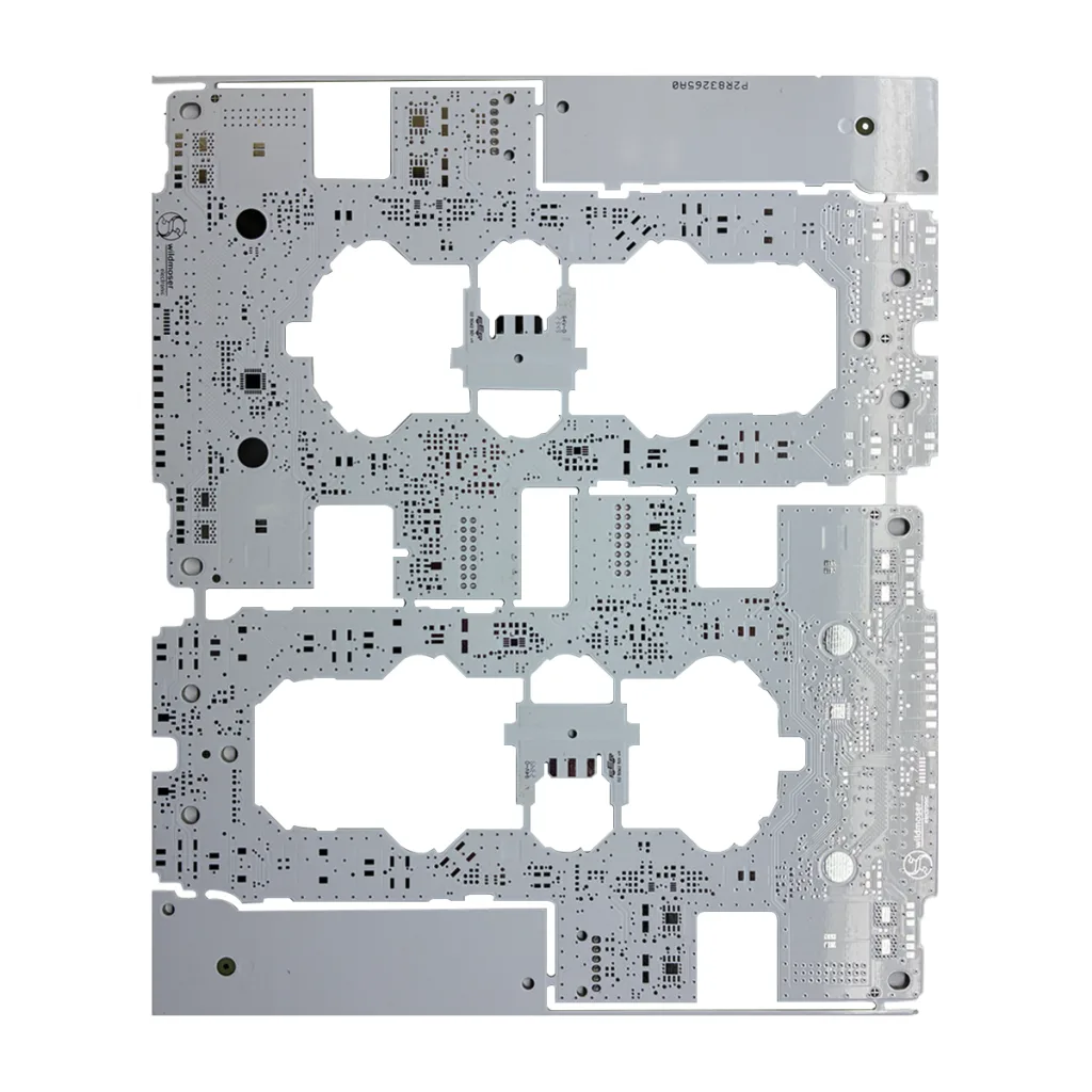
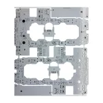
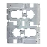
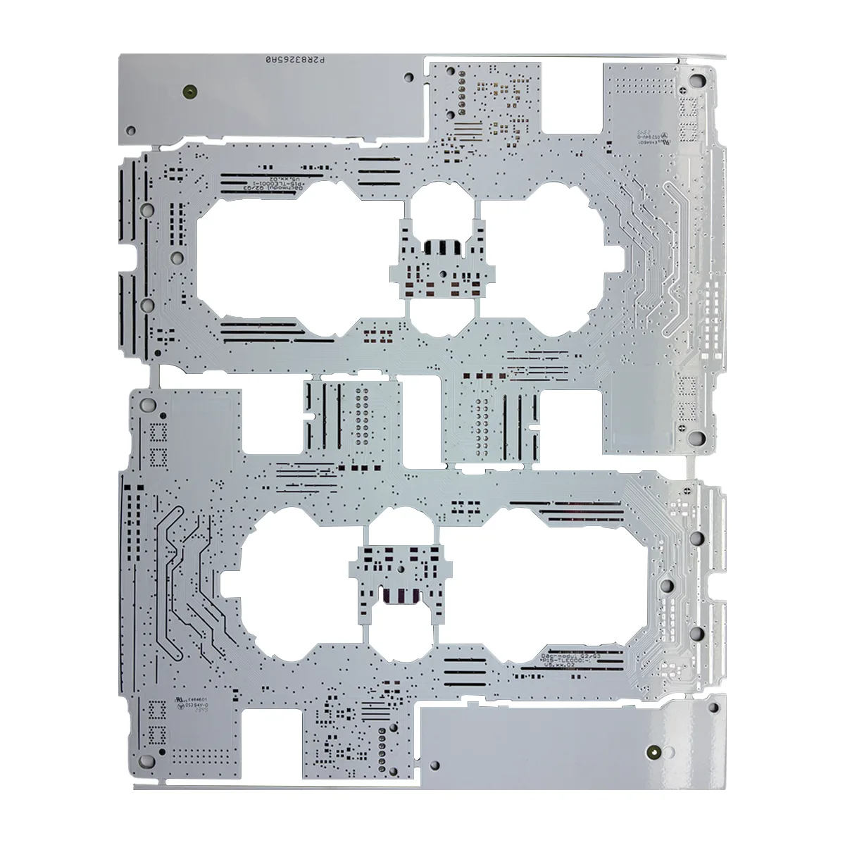
(Image Suggestion: Gallery of finished PCBs with different designs)
Alt Tag: Gallery of various 2 layer rigid PCB examples manufactured by UGPCB with white solder mask.


