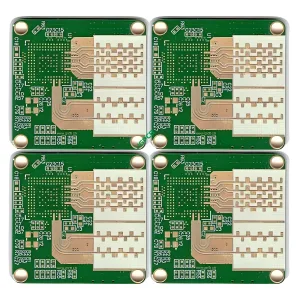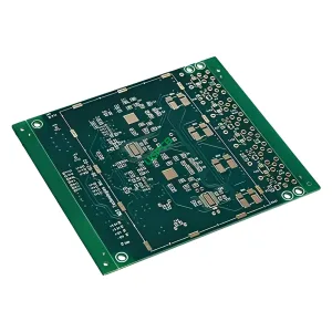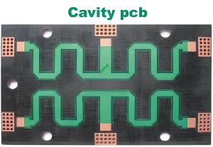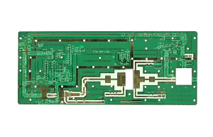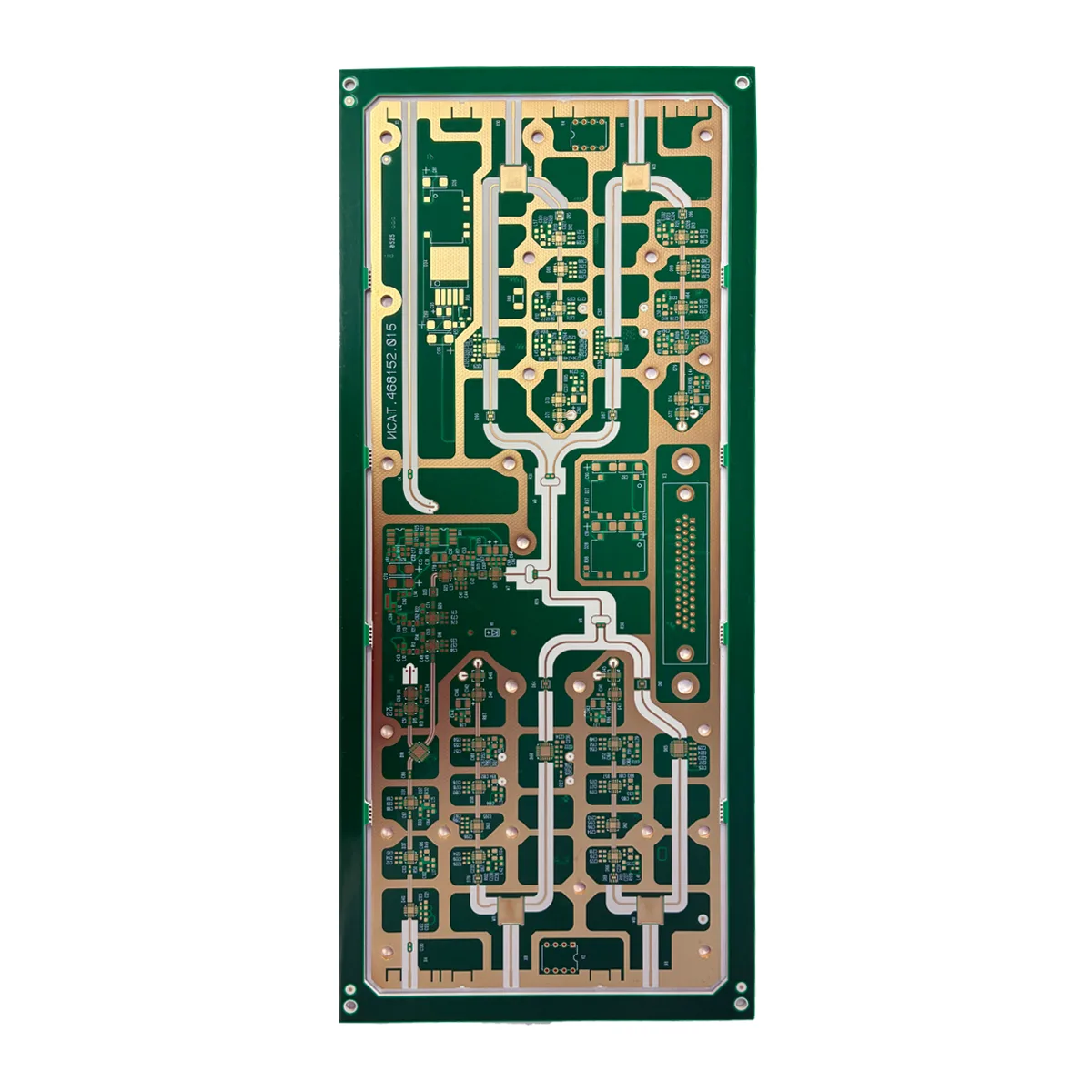
Professional 8-Layer Rogers 4350B High-Frequency PCB for Demanding RF & Microwave Applications
In the rapidly advancing fields of wireless communications, aeroespacial, and high-end test instrumentation, PCB padrão fall short of meeting extreme demands for signal integrity, baixa perda, and thermal stability. UGPCB leverages deep technical expertise to present this 8-Layer High-Frequency PCB construído em Rogers 4350B laminate. Engineered to address core challenges in RF applications, it is more than an interconnect—it’s a critical foundation ensuring stable performance and signal purity in advanced electronic systems.
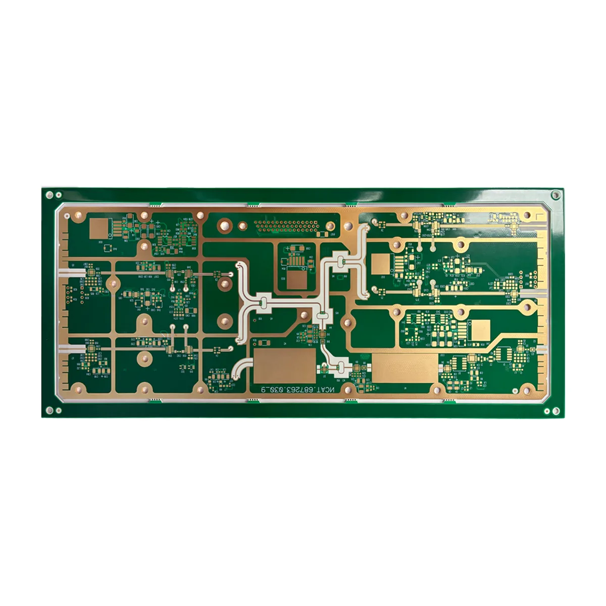
Visão geral do produto & Definição
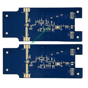
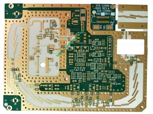
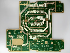
Este produto é um 8-camada rígida high-frequency Printed Circuit Board (PCB), utilizing the industry-recognized premium RF material—Rogers 4350b. Through precision multilayer lamination and specialized processing, it achieves high-density integration of complex RF circuits within a 1.65espessura da placa mm, delivering superior electrical performance control. It is specifically designed for applications requiring baixa perda, constante dielétrica estável, e excelente gerenciamento térmico.
Detailed Specifications & Considerações de design
Um produto de alta qualidade PCB starts with precise control over every detail. Below are the core specifications and their design significance:
| Categoria de parâmetro | Especificação | Justificativa do projeto & Implicação |
|---|---|---|
| Basic Structure | Camadas: 8 Camadas | Provides ample routing space, supports separate power, chão, and signal planes—essential for Interconexão de alta densidade (IDH) e Interferência Eletromagnética (EMI) suppression. |
| Espessura da placa: 1.65milímetros | A balanced thickness ensuring mechanical robustness and heat dissipation while accommodating spatial constraints in assemblies. | |
| Material central | Laminado: Rogers 4350b | The cornerstone of high-frequency Projeto de PCB. Its low dissipation factor (Df) e constante dielétrica estável (Dk) with minimal variation over frequency/temperature are critical for RF/microwave circuit integridade do sinal. |
| Condutividade | Peso de cobre: Interno 1/1 onças, Exterior 1/1 onças | Balanced copper weight ensures consistent current-carrying capacity and impedance control accuracy. 1 oz outer copper aids in heat dissipation. |
| Acabamento superficial | CONCORDAR (Ouro de imersão em níquel eletrolítico), 2eu” | Fornece um apartamento, highly solderable surface with excellent oxidation resistance, ensuring long-term reliability for RF connectors and BGA assemblies. |
| Dimensões Físicas | 280mm x 120 mm | Suited for medium-sized RF modules or subsystems, balancing integration density and mechanical strength. |
| Processos especiais | Depth-Controlled Milling (Step-down) + Vias Cegas | Key for enhanced spatial efficiency and performance. Step-down milling allows varied board heights; blind vias enable high-density interconnect from surface to inner layers, reducing signal crosstalk—a hallmark of advanced RF PCBs. |
Alt tag for suggested technical diagram: Cross-section diagram of 8-layer PCB stackup showing blind vias and step-down milling.
Como funciona & Aplicações primárias
Princípio de funcionamento:
Em altas frequências (MHz to GHz range), electrical signal transmission behaves more like electromagnetic wave propagation. This PCB leverages the stable dielectric properties of Rogers 4350B to provide a “smooth highway” for these waves, minimizing energy loss (perda de inserção) and waveform distortion during transmission. Its precise 8-layer stack-up e blind via design ensure controlled characteristic impedance (por exemplo, 50Ω or 75Ω) for transmission lines while mitigating interlayer signal reflection and crosstalk.
Principais aplicações:
-
Infraestrutura sem fio: 5G/6G base station antennas, amplificadores de potência (Não), filtros, LNAs.
-
Comunicações via satélite & Aeroespacial: Satellite transceiver modules, sistemas de radar, RF front-ends.
-
Teste de última geração & Medição: Core boards for network analyzers, analisadores de espectro, signal generators.
-
Eletrônica Automotiva: Millimeter-wave radar boards for ADAS.
-
Equipamento Médico: RF control modules in high-precision imaging systems (por exemplo, ressonância magnética).
Classificação Científica
Per industry and IPC standards, this product is classified as a Alta frequência, Multilayer Rigid Printed Circuit Board. More specifically, it is an 8-Layer Metal Core PCB with Blind Vias, fabricated on ceramic-filled hydrocarbon/glass weave reinforced laminate (Rogers 4350B series).
Construção & Key Performance Features
Análise Estrutural:
This PCB employs a classic symmetrical stack-up, comprising multiple signal layers with dedicated power and ground planes. Vias cegas connect the surface to adjacent inner layers, enquanto through-holes provide interconnection through the entire board. Depth-controlled milling creates mechanical recesses for shield can installation or special assembly requirements.
Outstanding Performance Features:
-
Perda de sinal ultrabaixa: The low dissipation factor of Rogers 4350b at GHz frequencies ensures high-efficiency signal transmission.
-
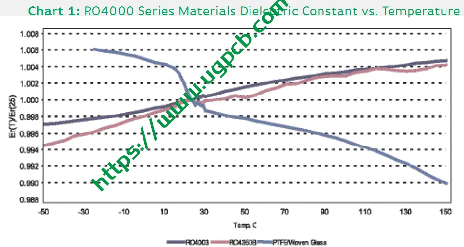
Exceptional Electrical Stability: Excellent thermal coefficient of dielectric constant (TCDk) guarantees consistent performance across a wide temperature range.
-
Gerenciamento térmico superior: Baixo coeficiente de expansão térmica (CTE) and high thermal conductivity enhance reliability in high-power RF circuits.
-
Controle de impedância de alta precisão: Achievable tolerance of ±5% or better, thanks to material stability and UGPCB’s advanced process control.
-
High-Reliability Interconnects: Robust 2μ” ENIG finish and precision blind via technology ensure durable connections in harsh environments.
-
Flexibilidade de design aprimorada: The combination of 8 camadas, vias cegas, and step milling supports highly complex and compact RF system design.
Core Manufacturing Process Flow
-
Preparação de material & Inner Layer Fabrication: Rogers 4350B clad laminates are sheared, perfurado (for blind vias), plated, patterned, and etched to form inner layer circuits.
-
Layup & Laminação: Etched inner layer cores and prepreg sheets are aligned in the designed stack-up and bonded under high temperature and pressure.
-
Perfuração Mecânica & Revestimento: Through-holes are drilled, followed by electroless and electrolytic copper plating to metallize all holes (PTH and blind vias).
-
Imagem da camada externa & Revestimento: Outer layer circuit pattern is applied, followed by pattern plating to build up trace and hole copper thickness.
-
Acabamento superficial: Ouro de imersão em níquel eletrolítico (CONCORDAR) process applied to form a 2-microinch nickel-gold protective layer on pads and hole walls.
-
CNC Routing & Step Milling: The board outline is routed, e depth-controlled milling creates step-down areas as per design.
-
Teste Elétrico & Inspeção: 100% teste elétrico (flying probe or fixture) for continuity and isolation, followed by final QA inspection (including impedance coupon testing).
Typical Use Case Scenarios
-
Cenário 1: 5G Massive MIMO Antenna Array Board
In such array boards, densely packed RF channels require minimal mutual interference. This PCB’s stable Dk and blind via design ensure channel isolation and phase coherence, while its superior thermal performance supports prolonged stable operation of PA chips.
Tudo telhado: 8-layer Rogers 4350B PCB assembly for a 5G Massive MIMO antenna unit. -
Cenário 2: Airborne Radar Signal Processing Front-End
Airborne environments involve large temperature swings and vibration. This PCB’s low TCDk ensures consistent radar performance across altitudes and temperatures, while the 1.65mm thick, robust construction resists vibrational stress.
Why Choose UGPCB for Your High-Frequency PCB?
-
Experiência em Materiais: We possess in-depth knowledge of processing high-frequency materials like Rogers, ensuring material integrity from storage through fabrication.
-
Capacidade Avançada de Processo: Mature processes for blind via registration e depth-controlled milling ensure first-pass success for complex designs.
-
Performance Validation: We provide critical impedance test reports e S-parameter data support using high-end network analyzers, bridging simulation and measurement.
-
Suporte de ponta a ponta: We offer full-cycle technical collaboration—from stack-up & impedance design, Análise DFM, to volume production—accelerating your time to market.
Ready to Power Your Next RF Project?
Contact a UGPCB engineer today for a comprehensive DFM review and a competitive quote. Submit your stack-up and impedance requirements to start the conversation.