

What is a 12L 2+N+2 HDI PCB?
A 12L 2+N+2 HDI PCB refers to a twelve-layer การเชื่อมต่อระหว่างกันที่มีความหนาแน่นสูง (HDI) แผงวงจรพิมพ์, featuring two core layers flanked by N signal layers and another two core layers. This configuration allows for high density interconnections, making it suitable for advanced electronic applications. ที่ “2+N+2” designation indicates the arrangement of the core and signal layers.
ข้อควรพิจารณาในการออกแบบ
Designing a 12L 2+N+2 HDI PCB involves several critical factors:
- การซ้อนชั้น: Proper alignment of the core and signal layers to ensure optimal electrical performance.
- ติดตามและพื้นที่: Minimal trace width and space of 3mil/3mil to accommodate fine features.
- Hole Sizes: Mechanical holes as small as 0.2mm and laser holes down to 0.1mm for precise component placement.
- ความหนาของทองแดง: Varied copper thickness with inner layers at 1OZ and outer layers at 0.5OZ to balance conductivity and flexibility.
มันทำงานอย่างไร?
The functionality of a 12L 2+N+2 เอชดีไอ พีซีบี relies on its multilayer structure and the use of high-density interconnects. Each layer serves a specific purpose:
- Core Layers: Provide structural integrity and act as the foundation for signal layers.
- Signal Layers: Carry electrical signals between components.
- การรักษาพื้นผิว: Immersion gold plus OSP ensures excellent solderability and long-term reliability by preventing oxidation.
การใช้งานและการจำแนกประเภท
 เหล่านี้ PCBS are primarily used in intelligent digital products where compact size and high performance are crucial. They can be classified based on their complexity and the number of layers, with the 12L 2+N+2 configuration being highly versatile for various applications.
วัสดุและประสิทธิภาพ
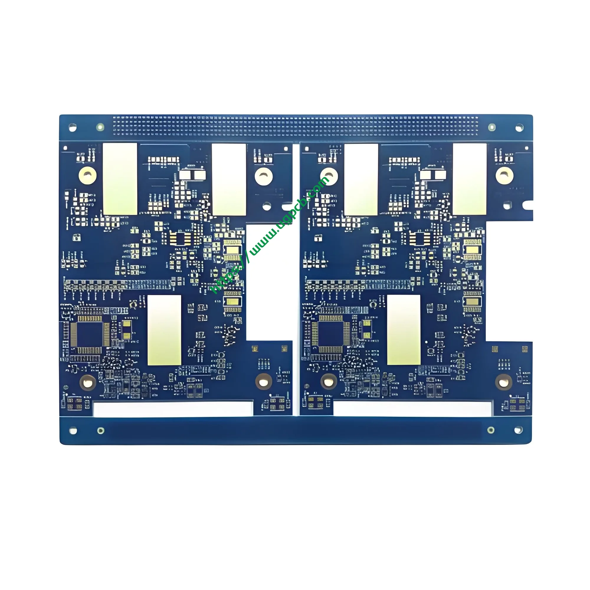
Constructed from FR-4 ITEQ, these PCBs offer excellent thermal stability and mechanical strength. The blue/white color scheme aids in visual inspection and troubleshooting. The finished thickness of 1.6mm provides a robust yet flexible board suitable for intricate designs.
โครงสร้างและคุณลักษณะ
The unique structure of a 12L 2+N+2 HDI PCB includes:
- Twelve Layers: Two core layers, N signal layers, and another two core layers.
- High Density Interconnects: Allow for complex routing and minimal space usage.
- การรักษาพื้นผิว: Immersion gold plus OSP enhances conductivity and protects against corrosion.
กระบวนการผลิต
The manufacturing process involves several sophisticated steps:
- การเตรียมวัสดุ: Selecting high-quality FR-4 substrate and copper foils.
- การซ้อนชั้น: Arranging the layers in a precise order to achieve the desired “2+N+2” configuration.
- พันธะ: การใช้ความร้อนและแรงกดเพื่อยึดชั้นต่างๆ เข้าด้วยกัน.
- การแกะสลัก: ใช้ etchant เพื่อขจัดทองแดงส่วนเกิน, เหลือเพียงเส้นทางนำไฟฟ้าที่ต้องการ.
- การชุบ: Adding a thin layer of metal to improve conductivity and solderability.
- การรักษาพื้นผิว: Applying immersion gold plus OSP to protect against oxidation and enhance solderability.
- การควบคุมคุณภาพ: ดำเนินการตรวจสอบและทดสอบอย่างละเอียดเพื่อให้แน่ใจว่าบอร์ดแต่ละบอร์ดมีคุณสมบัติตรงตามมาตรฐานคุณภาพที่เข้มงวด.

กรณีการใช้งานและสถานการณ์
12L 2+N+2 HDI PCBs are ideal for use in intelligent digital products where miniaturization and high performance are critical. แอปพลิเคชันทั่วไปรวมถึง:
- สมาร์ทโฟน: ช่วยให้มีการออกแบบที่เพรียวบางขึ้นโดยไม่กระทบต่อฟังก์ชันการทำงานหรือประสิทธิภาพ.
- เม็ด: ให้การเชื่อมต่อที่เชื่อถือได้สำหรับการถ่ายโอนและประมวลผลข้อมูลความเร็วสูง.
- อุปกรณ์สวมใส่ได้: รองรับการออกแบบที่กะทัดรัดในขณะที่ยังคงประสิทธิภาพและความทนทานที่แข็งแกร่ง.
- เครื่องเล่นมีเดียแบบพกพา: รับประกันความสามารถในการประมวลผลเสียงและวิดีโอคุณภาพสูงในรูปแบบขนาดเล็ก.
สรุปแล้ว, the 12L 2+N+2 HDI PCB represents a pinnacle of innovation in PCB technology, ให้ความหนาแน่นที่ไม่มีใครเทียบได้, ผลงาน, และความน่าเชื่อถือสำหรับแอปพลิเคชันอิเล็กทรอนิกส์สำหรับผู้บริโภคที่มีความต้องการมากที่สุด.


