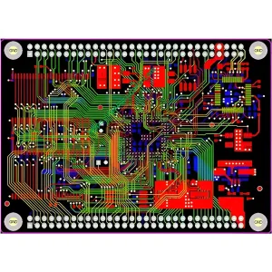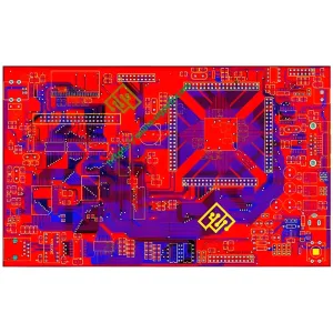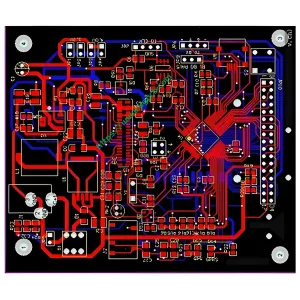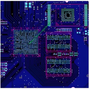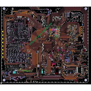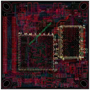
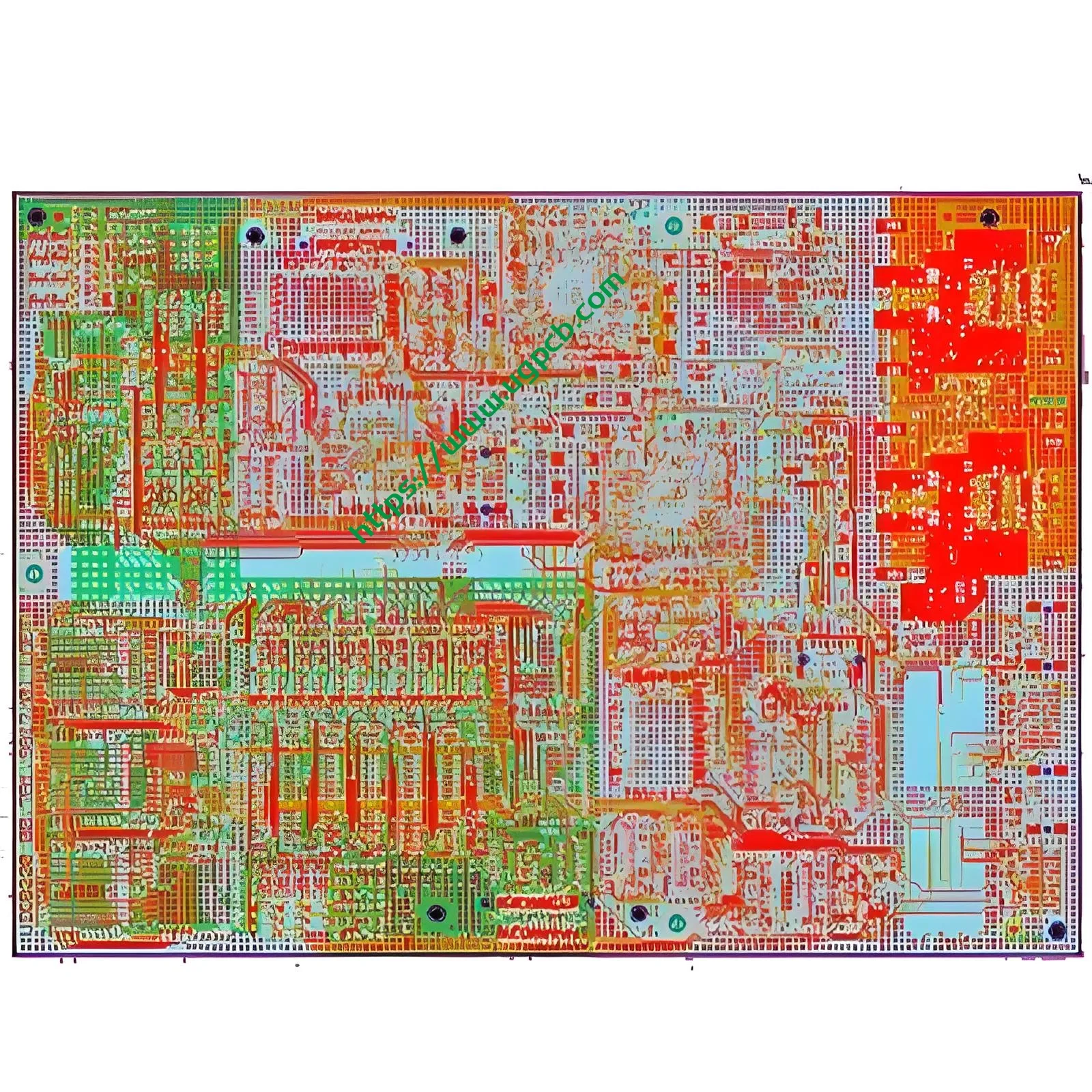
Overview of 16-Layer Stack PCB
A 16-layer stack has 16 layers of routing and is typically used for high-density designs.
Routing Challenges and Solutions
Routing Challenges
In EDA applications, routing techniques often fail to route the design.
สารละลาย: Adding Multiple Layers
That’s why manufacturers add multiple layers to accommodate the complexity of high-density designs.
Specifications of 16-Layer PCB Fabrication
องค์ประกอบ
- Made of 16 ชั้น
- Made of halogen-free materials, อลูมิเนียม, CEM, และ FR
ความหนาของแผ่น
- Extended to 7 มม
ขนาดกระดาน
- Maximum finished board size is 500 x 500 มม
เสร็จสิ้น
- Halogen-free gold and silver plated
UGPCB: High-Quality Fabrication
UGPCB offers high-quality fabrication of 16-layer stack PCBs, ensuring reliability and performance for high-density designs.